3916デジタルインフォメーションテクノロジー(株)[DIT]
市場:東証PRM
業種:情報通信業
デジタル・インフォメーション・テクノロジーズ株式会社は、主にソフトウェア開発事業とシステム販売事業を行う日本の会社です。同社は 2 つの事業セグメントを通じて事業を展開しています。ソフトウェア開発事業は、業務システム開発事業や運用支援事業などのビジネスソリューション事業、組み込み開発事業や組み込み検証事業などの組み込みソリューション事業、サイバーセキュリティ製品やビジネスオートメーション製品などを提供するプロダクト事業を行っております。システム販売事業は、主に中小企業向け経営支援基幹システム製品「楽一」の販売を行っております。
関連: システムインテグレーション/IT/SaaS/自動運転車/フィンテック/IoT/サイバーセキュリティ/RPA/コネクテッドカー/ERP/Society5.0/人工知能/デジタルトランスフォーメーション/業務支援/ポストコロナ/金融向けシステム
スポンサード リンク
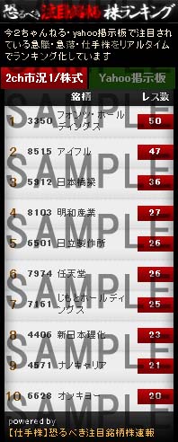
デジタル・インフォメーション・テクノロジー(3916)時間別の2ch&Yahoo投稿数推移(48時間)
スポンサード リンク
- 全て表示
- 関連ブログ情報
- 【2ch】市況1/株式板(5ch)
- 【Yahoo】ファイナンス掲示板
- twitter呟き
- [3916]デジタル・インフォメーション・テクノロジー 株式掲示板
関連ブログ情報 新着リスト
-
-
 2026/04/12 PR
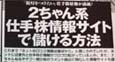
【3916】DITをまだ握ってる人は手離すべき?!最新技術と方法な知識で次世代型の投資戦略をご提案!
2026/04/12 PR
【3916】DITをまだ握ってる人は手離すべき?!最新技術と方法な知識で次世代型の投資戦略をご提案!
- プレナスでは最新AIを用いることで膨大なデータ量を人間では不可能な速度で分析・判断が可能です。人力をメインとする投資顧問では…
- https://plenus-investment.com/
-
-
-
2025/12/03
値上がり予想銘柄API-1(不定期)(2025,12,2)
- 値上がり予想銘柄API-1(不定期)(2025,12,2) - 値上がり予想銘柄API-1(不定期)(2025,12,2) 3359 cotta 3916 デジタル・インフォメーション・テクノロジー 6440 JUKI 7358 ポピンズ 投資は自己判断で! #株 #株投資...
- https://kabu-chan11.muragon.com/entry/7527.html
-
-
-
2025/12/03
値上がり予想銘柄2(API_Rank1)(2025,12,2)
- 値上がり予想銘柄2(API_Rank1)(2025,12,2) - 値上がり予想銘柄2(API_Rank1)(2025,12,2) 2286 林兼産業 3359 cotta 3916 デジタル・インフォメーション・テクノロジー 5033 ヌーラボ 6195 ホープ 6440...
- https://kabu-chan11.muragon.com/entry/7524.html
-
-
-
2025/11/14
[株式分割情報] デジタル・インフォメーション・テクノロジー(3916) 1株⇒2株
- [株式分割情報] デジタル・インフォメーション・テクノロジー(3916) 1株⇒2株,株入門初心者におすすめ!!株価が騰がる買い方始め方タイミングを予想しチャンスを逃さない投資無料ブログ。経済指標のビッグデータ解析と機械学習によるオリジナル予測理論!!NYダウ&日経平均株価予想(先物)を算出!! リーマンショック級暴落事前予想も!!当たる確率は80%!!株式分割・東証1部昇格・格付け情報も!!
- https://senkouyosoku.seesaa.net/article/518946054.html
-
【2ch】市況1板、株式板の反応(新着順)
スポンサード リンク
【急騰】今買えばいい株26768【含み損×ト×忍耐】より
5 :山師さん:2026/04/07(火)20:52:07 ID:ejO9ZSJ7.net
【急騰】今買えばいい株26762【トランプの極意】より
736 :山師さん:2026/04/07(火)02:18:55 ID:FzQdJjeu.net
He has refused his Assent to Laws, the most wholesome and necessary for the public good.
He has forbidden his Governors to pass Laws of immediate and pressing importance, unless suspended in their operation till his Assent should be obtained; and when so suspended, he has utterly neglected to attend to them.
He has refused to pass other Laws for the accommodation of large districts of people, unless those people would relinquish the right of Representation in the Legislature, a right inestimable to them and formidable to tyrants only.
He has called together legislative bodies at places unusual, uncomfortable, and distant from the depository of their public Records, for the sole purpose of fatiguing them into compliance with his measures.
He has dissolved Representative Houses repeatedly, for opposing with manly firmness his invasions on the rights of the people.
He has refused for a long time, after such dissolutions, to cause others to be elected; whereby the Legislative powers, incapable of Annihilation, have returned to the People at large for their exercise; the State remaining in the mean time exposed to all the dangers of invasion from without, and convulsions within.
He has endeavoured to prevent the population of these States; for that purpose obstructing the Laws for Naturalization of Foreigners; refusing to pass others to encourage their migrations hither, and raising the conditions of new Appropriations of Lands.
He has obstructed the Administration of Justice, by refusing his Assent to Laws for establishing Judiciary powers.
He has made Judges dependent on his Will alone, for the tenure of their offices, and the amount and payment of their salaries.
He has erected a multitude of New Offices, and sent hither swarms of Officers to harrass our people, and eat out their substance.
He has kept among us, in times of peace, Standing Armies without the Consent of our legislatures.
He has affected to render the Military independent of and superior to the Civil power.
He has combined with others to subject us to a jurisdiction foreign to our constitution, and unacknowledged by our laws; giving his Assent to their Acts of pretended Legislation:
For Quartering large bodies of armed troops among us:
For protecting them, by a mock Trial, from punishment for any Murders which they should commit on the Inhabitants of these States:
For cutting off our Trade with all parts of the world:
For imposing Taxes on us without our Consent:
For depriving us in many cases, of the benefits of Trial by Jury:
For transporting us beyond Seas to be tried for pretended offences:
For abolishing the free System of English Laws in a neighbouring Province, establishing therein an Arbitrary government, and enlarging its Boundaries so as to render it at once an example and fit instrument for introducing the same absolute rule into these Colonies:
For taking away our Charters, abolishing our most valuable Laws, and altering fundamentally the Forms of our Governments:
For suspending our own Legislatures, and declaring themselves invested with power to legislate for us in all cases whatsoever.
He has abdicated Government here, by declaring us out of his Protection and waging War against us.
He has plundered our seas, ravaged our Coasts, burnt our towns, and destroyed the lives of our people.
He is at this time transporting large Armies of foreign Mercenaries to compleat the works of death, desolation and tyranny, already begun with circumstances of Cruelty & perfidy scarcely paralleled in the most barbarous ages, and totally unworthy the Head of a civilized nation.
He has constrained our fellow Citizens taken Captive on the high Seas to bear Arms against their Country, to become the executioners of their friends and Brethren, or to fall themselves by their Hands.
【急騰】今買えばいい株26762【トランプの極意】より
727 :山師さん:2026/04/07(火)02:14:57 ID:HCeMYOna.net
We-the President of the United States, the President of the National Government of the Republic of China, and the Prime Minister of Great Britain, representing the hundreds of millions of our countrymen, have conferred and agree that Japan shall be given an opportunity to end this war.
The prodigious land, sea and air forces of the United States, the British Empire and of China, many times reinforced by their armies and air fleets from the west, are poised to strike the final blows upon Japan. This military power is sustained and inspired by the determination of all the Allied Nations to prosecute the war against Japan until she ceases to resist.
The result of the futile and senseless German resistance to the might of the aroused free peoples of the world stands forth in awful clarity as an example to the people of Japan. The might that now converges on Japan is immeasurably greater than that which, when applied to the resisting Nazis, necessarily laid waste to the lands, the industry and the method of life of the whole German people. The full application of our military power, backed by our resolve, will mean the inevitable and complete destruction of the Japanese armed forces and just as inevitably the utter devastation of the Japanese homeland.
The time has come for Japan to decide whether she will continue to be controlled by those self-willed militaristic advisers whose unintelligent calculations have brought the Empire of Japan to the threshold of annihilation, or whether she will follow the path of reason.
Following are our terms. We will not deviate from them. There are no alternatives. We shall brook no delay.
There must be eliminated for all time the authority and influence of those who have deceived and misled the people of Japan into embarking on world conquest, for we insist that a new order of peace, security and justice will be impossible until irresponsible militarism is driven from the world.
Until such a new order is established and until there is convincing proof that Japan's war-making power is destroyed, points in Japanese territory to be designated by the Allies shall be occupied to secure the achievement of the basic objectives we are here setting forth.
The terms of the Cairo Declaration shall be carried out and Japanese sovereignty shall be limited to the islands of Honshu, Hokkaido, Kyushu, Shikoku and such minor islands as we determine.
The Japanese military forces, after being completely disarmed, shall be permitted to return to their homes with the opportunity to lead peaceful and productive lives.
We do not intend that the Japanese shall be enslaved as a race or destroyed as a nation, but stern justice shall be meted out to all war criminals, including those who have visited cruelties upon our prisoners. The Japanese Government shall remove all obstacles to the revival and strengthening of democratic tendencies among the Japanese people. Freedom of speech, of religion, and of thought, as well as respect for the fundamental human rights shall be established.
Japan shall be permitted to maintain such industries as will sustain her economy and permit the exaction of just reparations in kind, but not those which would enable her to re-arm for war. To this end, access to, as distinguished from control of, raw materials shall be permitted. Eventual Japanese participation in world trade relations shall be permitted.
The occupying forces of the Allies shall be withdrawn from Japan as soon as these objectives have been accomplished and there has been established in accordance with the freely expressed will of the Japanese people a peacefully inclined and responsible government.
We call upon the government of Japan to proclaim now the unconditional surrender of all Japanese armed forces, and to provide proper and adequate assurances of their good faith in such action. The alternative for Japan is prompt and utter destruction.
板別にレスを表示する
![]()

Yahoo掲示板(Y板)の反応(新着順)
スポンサード リンク
2026/04/11(土) 21:16:00投稿者:波乗りジョニー
人海戦術でする設定やバグ発見とか、もう・・・・・・泣、、一時は、10年増収増配ってキャッチだったけれども、次回の5月15日の第三四半期決算で通期見通しどうなるか、、
2026/04/10(金) 21:19:00投稿者:伊右衛門
経営者は株価が上がるよう業績をあげるなり、将来の施策を打つのが仕事です
株価が上がらなければ株主は「文句」を言うのが自然の流れだと思います
2026/04/10(金) 20:58:00投稿者:瑜吉
ここで文句言ってても株価は上がらないし、むしろ逆効果だと思うので株価が下がってイライラして文句言うぐらいなら損切りして他の銘柄買った方が精神的にもいいんじゃないかと思っただけです。
空売りの可能性もあるので「もし」をつけました。
2026/04/10(金) 20:30:00投稿者:伊右衛門
会社の経営者は「文句があるならさっさと株を売ればいい」なんてこと、まさか言わないと思いますが・・
株主の意見を真摯に聞いて欲しいですね
2026/04/10(金) 20:09:00投稿者:伊右衛門
会社関係者の投稿もあると思います
「文句があるならさっさと売ってしまえ」なんて投稿ごあるなら、それこそ株主をバカにしている他ないと思います
2026/04/10(金) 14:02:00投稿者:伊右衛門
経営者の努めは株主に対していろいろな形で還元することだと思います
ここは最近それが出来てないから多くの人が意見を言いたくなるのでは?
その中には文句があって当たり前ではないでしょうか?
2026/04/10(金) 10:05:00投稿者:瑜吉
もしここの株持ってるならさっさと売ってスッキリすれば、文句言わなくて済みますよ。
2026/04/10(金) 09:58:00投稿者:素人
ブラック!ブラック!ブラック!
人材が辞めるので、、
株価はさがるのみ‼️
2026/04/10(金) 09:34:00投稿者:伊右衛門
800台も冗談じゃなくなってきたぞ!
株価が上がると誰か困るんかい
イッチー!
2026/04/09(木) 17:12:00投稿者:zer*****
この株は長期保有の我慢料が相当溜まっていますね。
永く持てる人が大きな我慢料を手に入れるんでしょうね。
twitter検索
|
|
IRSTREET_JP
デジタル・インフォメーション・テクノロジー(3916) 藤田医科大学病院の屋内配送向けトライアルサービスのプラットフォームクラウドシステムの共同開発者として紹介されました https://t.co/IOaNtsqARf |
|---|
|
|
karauriNET
Merrill Lynch internationalの空売り残高(7/7)
3853 アステリア 0.5% 再IN
3900 クラウドワークス -0.04%
3911 Aiming -0.05%
3916 デジタル・インフォメ… https://t.co/nzwzH1uFOP |
|---|
|
|
karimeropipipi
ご登壇3社
✨DIT デジタル・インフォメーション・テクノロジー(3916)
✨ランドコンピュータ(3924)
✨PCIホールディングス(3918)
3社とも情報通信業、かつB to B事業が中心なので今まであまり馴染みのない会社👀
本日の動画は後ほど公開予定だそうです |
|---|
|
|
BridgeSalon
■本日公開のブリッジレポート
デジタル・インフォメーション・テクノロジー株式会社(3916)
「業績下方修正 増配予想は維持」
本文は以下よりご覧いただけます。
https://t.co/WkxeUQCna3
#投資 #プライム |
|---|
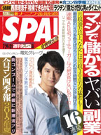
 週刊SPA!7/24・31合併号のマネー(得)総本部のコーナーで当サイト『恐るべき注目銘柄株速報』のインタビュー記事が掲載されました。
We-the President of the United States, the President of the National Government of the Republic of China, and the Prime Minister of Great Britain, representing the hundreds of millions of our countrymen, have conferred and agree that Japan shall be given an opportunity to end this war.
The prodigious land, sea and air forces of the United States, the British Empire and of China, many times reinforced by their armies and air fleets from the west, are poised to strike the final blows upon Japan. This military power is sustained and inspired by the determination of all the Allied Nations to prosecute the war against Japan until she ceases to resist.
The result of the futile and senseless German resistance to the might of the aroused free peoples of the world stands forth in awful clarity as an example to the people of Japan. The might that now converges on Japan is immeasurably greater than that which, when applied to the resisting Nazis, necessarily laid waste to the lands, the industry and the method of life of the whole German people. The full application of our military power, backed by our resolve, will mean the inevitable and complete destruction of the Japanese armed forces and just as inevitably the utter devastation of the Japanese homeland.
The time has come for Japan to decide whether she will continue to be controlled by those self-willed militaristic advisers whose unintelligent calculations have brought the Empire of Japan to the threshold of annihilation, or whether she will follow the path of reason.
Following are our terms. We will not deviate from them. There are no alternatives. We shall brook no delay.
There must be eliminated for all time the authority and influence of those who have deceived and misled the people of Japan into embarking on world conquest, for we insist that a new order of peace, security and justice will be impossible until irresponsible militarism is driven from the world.
Until such a new order is established and until there is convincing proof that Japan's war-making power is destroyed, points in Japanese territory to be designated by the Allies shall be occupied to secure the achievement of the basic objectives we are here setting forth.
The terms of the Cairo Declaration shall be carried out and Japanese sovereignty shall be limited to the islands of Honshu, Hokkaido, Kyushu, Shikoku and such minor islands as we determine.
The Japanese military forces, after being completely disarmed, shall be permitted to return to their homes with the opportunity to lead peaceful and productive lives.
We do not intend that the Japanese shall be enslaved as a race or destroyed as a nation, but stern justice shall be meted out to all war criminals, including those who have visited cruelties upon our prisoners. The Japanese Government shall remove all obstacles to the revival and strengthening of democratic tendencies among the Japanese people. Freedom of speech, of religion, and of thought, as well as respect for the fundamental human rights shall be established.
Japan shall be permitted to maintain such industries as will sustain her economy and permit the exaction of just reparations in kind, but not those which would enable her to re-arm for war. To this end, access to, as distinguished from control of, raw materials shall be permitted. Eventual Japanese participation in world trade relations shall be permitted.
The occupying forces of the Allies shall be withdrawn from Japan as soon as these objectives have been accomplished and there has been established in accordance with the freely expressed will of the Japanese people a peacefully inclined and responsible government.
We call upon the government of Japan to proclaim now the unconditional surrender of all Japanese armed forces, and to provide proper and adequate assurances of their good faith in such action. The alternative for Japan is prompt and utter destruction.