

スポンサード リンク
- 全て表示
- 関連ブログ情報
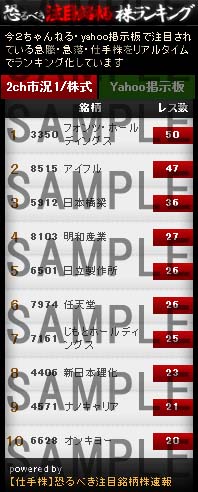
- 【2ch】市況1/株式板(5ch)
- 【Yahoo】ファイナンス掲示板
- twitter呟き
- [300]MIC 株式掲示板
関連ブログ情報 新着リスト
-
-
 2026/04/06 PR
MIC(300)は大丈夫?あの株界レジェンドが今強く警告している大化け銘柄とは…
2026/04/06 PR
MIC(300)は大丈夫?あの株界レジェンドが今強く警告している大化け銘柄とは…
- 20年以上の長きにわたり数多くの大化け銘柄を排出し続け「神がかり」とまで言われる相場界のレジェンド。そしてラジオNIKKEIでもお馴染みの…
- https://shinseijapan.com/
-
-
-
2026/03/20
銘柄:300A MIC
- 優良銘柄の紹介しています。今回は、 銘柄:300A MIC です。- 注目 -・自己資本比率 70 %以上・利益剰余金 - 有利子負債 が、黒字・キャッシュフロー(CF)残高 黒字・出来高 7600 株 / 日・増配 1. 株式情報※会社四季報(2026年1集)より、抜粋~~…
- https://moneyholder.seesaa.net/article/520153492.html
-
-
-
2026/02/13
決算AIを”アナリスト”に昇格させる ── Claude vs Geminiに「買い?」と聞いたら評価が割れた【MIC(300A)で検証】
- 決算要約AIに「A-D評価とエントリー助言」を聞いたらどうなる? MIC(300A)3Q決算でClaude Opus 4.6とGemini 3.0 Proを比較。検索行動・評価・中立性の違いと、翌日株価での答え合わせを公開。
- https://gamerinvestlog.com/claude-gemini-investment-analyst-rating/
-
-
-
2025/11/14
東証スタンダード(前引け)=値下がり優勢、エスクリ、コスモバイオがS高
- 14日前引けの東証スタンダード市場は値上がり銘柄数525、値下がり銘柄数833と、値下がりが優勢だった。 個別ではエスクリ、コスモ・バイオがストップ高。MIC、児玉化学
- https://stock.f-frontier.com/2025/11/14/227957/
-
【2ch】市況1板、株式板の反応(新着順)
スポンサード リンク
【急騰】今買えばいい株26677【優待ただ鳥】より
404 :山師さん:2026/03/22(日)10:17:52 ID:mS9WhFVM.net
【急騰】今買えばいい株26672【小春日和】より
891 :山師さん:2026/03/20(金)19:56:27 ID:5xQXd1dj.net
「OpenAIは死んだ」とのAlgorithmic Bridgeのポスト😱
1. 信頼喪失:DoD問題でブランド毀損(企業の信頼低下)
2. 競合:企業向けでAnthropicに逆転され売上でも抜かれる見込み
3. 資金支援者:Microsoftとの決定的な関係悪化
4. インフラ: Stargate計画始まらず
5. 戦略:チップやデバイスなど多方面に分散
6. 訴訟:イーロンマスクとの闘争
7. 財務:巨額赤字継続
ここに社運かけるレベルで投資してるとこあったな
【急騰】今買えばいい株26603【日経-50,000】より
484 :山師さん:2026/03/19(木)22:20:33 ID:XBicgxWl.net
ホワイトハウス情報セキュリティ顧問カミロサンドバルのツイート
これ日本が海上保険トランジットしろいうてる?
𝗧𝗿𝘂𝗺𝗽 𝗠𝗮𝘆 𝗣𝗿𝗲𝘀𝘀 𝗝𝗮𝗽𝗮𝗻 𝗳𝗼𝗿 𝗦𝘂𝗽𝗽𝗼𝗿𝘁 𝗼𝗻 𝗜𝗿𝗮𝗻 𝗗𝘂𝗿𝗶𝗻𝗴 𝗧𝗼𝗱𝗮𝘆’𝘀 𝗪𝗵𝗶𝘁𝗲 𝗛𝗼𝘂𝘀𝗲 𝗠𝗲𝗲𝘁𝗶𝗻𝗴:
The ongoing disruptions in the Strait of Hormuz are both economic and military in nature. Shipping has been constrained not only by security threats and vessel damage, but by surging insurance costs that have effectively priced many operators out of transit.
Rather than relying solely on military deployments, Japan is uniquely positioned to play a decisive economic role in stabilizing the situation.
One compelling solution would be for the Bank of Japan to establish a sovereign-backed reinsurance facility for vessels transiting the Strait—potentially anchored by a $50 billion commitment to absorb risk and restore market confidence. This would build on the $20 billion reinsurance framework initially established under President Trump, scaling it into a far more powerful instrument with a meaningful value-multiplier effect across global shipping and energy markets.
【急騰】今買えばいい株26646【日経の逆襲】より
76 :山師さん:2026/03/16(月)09:30:29 ID:gl5BebDN.net
>化学工業日報社@chemicaldailyad·18時間
>ホルムズ海峡の事実上の封鎖を受け、国内石油化学業界ではナフサ分解炉(エチレン設備)の稼働を一部停止するリスクが現実味を帯びてきた。原料となる中東産ナフサの調達難により設備の稼働を引き下げる対策が広がるなか、一部企業では操業停止を計画していることがわかった。
大変な事になりそう
【急騰】今買えばいい株26636【ガソリンの買いかた】より
157 :山師さん:2026/03/13(金)09:15:09 ID:2zaA0Wtd.net
IRGC Reports Strike On USS Abraham Lincoln.
Iran’s Islamic Revolutionary Guard Corps states that missiles and drones targeted the U.S. aircraft carrier USS Abraham Lincoln, reportedly causing significant damage.
リンカーンにねてー
板別にレスを表示する
![]()

Yahoo掲示板(Y板)の反応(新着順)
スポンサード リンク
2026/03/30(月) 13:09:00投稿者:1b8*****
大注目の銘柄ですわ
2026/03/18(水) 12:49:00投稿者:kur*****
四季報プロ500に取り上げられると、株価下がるんだよな。
2026/03/17(火) 13:24:00投稿者:肉損は暇人
ここ数日の出来高も良い感じ
2026/03/10(火) 12:19:00投稿者:spf*****
運送業・・・・苦笑
2026/03/10(火) 11:43:00投稿者:spf*****
運送業・・・苦笑
2026/03/10(火) 09:19:00投稿者:7750000
燃料高は運送業には間違いなくマイナスだからね。
2026/03/09(月) 00:10:00投稿者:f7d*****
退職後に株を始めたけれど、なかなか結果が出ず、
悩んでいた私が、毎朝届く情報を受け取るようになってから、
気づけば+32%の利益!✨
最初は半信半疑でしたが、理由も納得できました。
無料で受け取れるので、今すぐチェックしてみてください!
無料配信中の投資情報
2026/03/08(日) 01:02:00投稿者:3f1*****
個別株で安定して勝つのは難しい。
そう感じている方へ。
私はある無料株式グループに参加し、
毎朝の情報を参考にしています。
売買ポイントまで提示。
先月+37%。
興味がある方は、
2026/03/06(金) 23:50:00投稿者:LT
嬉しいことだけど、なんかあった?
2026/03/06(金) 23:21:00投稿者:726*****
相場環境は悪くない。
それでも安定して利益を積み重ねるのは簡単ではありません。
私はこれまで、感覚的な売買で何度も失敗してきました。
今年から参加している株式グループでは、
毎朝7時に戦略銘柄が共有されます。
・中長期で成長が期待できる銘柄
・短期急騰を狙うテーマ株
・高配当の安定銘柄
そして具体的な売買目安。
感情に左右される取引が大幅に減りました。
先月は+37%。
驚いたのは、
これらの情報が完全無料で提供されていること。
興味がある方は、
twitter検索
エラーが発生しました。
300 MIC(株) ツイッター株予想よりご覧ください


 週刊SPA!7/24・31合併号のマネー(得)総本部のコーナーで当サイト『恐るべき注目銘柄株速報』のインタビュー記事が掲載されました。
>>393
ここは最新の主流データ(主に**International IQ Testの2026年更新版、2025年の1,212,714人サンプルに基づくもの
**Average IQ Ranking by Country (2026)**
1. South Korea — 106.97
2. China — 106.48
3. Japan — 106.3
4. Iran (Islamic Republic of) — 104.8
(出典: international-iq-test.com/en/test/IQ_by_country、2026年1月1日更新。参加者数: Iran 10,538人)