

4319TAC(株)
市場:東証STD
業種:サービス業
株式会社タック主に教育サービスの提供に従事しています。個別教育部門では、公認会計士、税理士、不動産鑑定士、社会保険労務士、証券アナリスト、情報処理技術者等の資格試験の試験対策を実施しています。法人研修事業は、企業、大学、専門学校、会計事務所等を対象とした資格取得等に関する研修・講座の提供、学習教材の提供及びコンサルティングサービス、税務申告ソフトの販売、提携スクールの展開等の事業を行っております。出版事業では、教育関連書籍の出版を行っております。人材事業は、人材紹介・人材派遣サービスの提供及びインターネットを通じた求人サイトの運営を行っております。
関連: 資格学校/eラーニング/アベノミクス/サマータイム/人材紹介/出版/人生100年時代/あえてスタンダード/サービス業
上場廃止
スポンサード リンク
スポンサード リンク
- 全て表示
- 関連ブログ情報
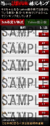
- 【2ch】市況1/株式板(5ch)
- 【Yahoo】ファイナンス掲示板
- twitter呟き
- [4319]TAC 株式掲示板
関連ブログ情報 新着リスト
-
-
 2026/04/07 PR
TAC(4319)は大丈夫?あの株界レジェンドが今強く警告している大化け銘柄とは…
2026/04/07 PR
TAC(4319)は大丈夫?あの株界レジェンドが今強く警告している大化け銘柄とは…
- 20年以上の長きにわたり数多くの大化け銘柄を排出し続け「神がかり」とまで言われる相場界のレジェンド。そしてラジオNIKKEIでもお馴染みの…
- https://shinseijapan.com/
-
-
-
2025/09/03
4319yu
- 4319:TAC おすすめ度:2 最低投資金額:34,900円 配当利回り 2% 優待利回り 0% 2025.9.1の株価情報にて反映 資格関係の大手です。開講講座の受講料の割引券を貰えます。 今回はTACの株主優待について紹介したいと思い
- https://kabumura.com/4319yu/
-
-
-
2025/08/09
4319TACが350円でMBOされます。
- 資格の学校でお馴染みの4319TACさんが創業家によるTOBを実施されます。6日の終値239円より46%アップのTOB価格は350円との事です。既に8日の終値…
- https://ameblo.jp/m195617/entry-12921733712.html
-
-
-
2025/08/07
東証スタンダード(大引け)=値上がり優勢、協立情報通信、TACがS高
- 7日大引けの東証スタンダード市場は値上がり銘柄数855、値下がり銘柄数551と、値上がりが優勢だった。 個別では協立情報通信、TAC、ソフト99コーポレーション、安永&
- https://stock.f-frontier.com/2025/08/07/219866/
-
【2ch】市況1板、株式板の反応(新着順)
スポンサード リンク
【急騰】今買えばいい株26019【ハゲ市早苗】より
857 :山師さん:2025/10/22(水)11:30:48 ID:fj4+ABAY.net
【急騰】今買えばいい株26019【ハゲ市早苗】より
741 :山師さん:2025/10/22(水)11:15:54 ID:jKukeDhC.net
=== 独走状態入った ===
50 ID:0tI7dyqq
22 ID:W6VGvCEt
21 ID:V70C3the
19 ID:AeeNowQz
19 ID:gLd8KY7Y
15 ID:vH/j6VCc
14 ID:kdQUV6y/
14 ID:bSBoFbfD
12 ID:WsShQOsN
11 ID:OH0p+TAc
11 ID:denTIfe3
11 ID:/ocV7W2U
【急騰】今買えばいい株26019【ハゲ市早苗】より
94 :山師さん:2025/10/22(水)10:14:30 ID:GuKXMvcl.net
=== 前スレランキング ===
36 ID:eYxaxSa+
36 ID:TpIQ2/9i
25 ID:V8CR8gJd
18 ID:OH0p+TAc
17 ID:tRA5uD6v
17 ID:OEMaAq6t
15 ID:by4kSQ2B
15 ID:YVPNsfH5
14 ID:VZEUxYu2
14 ID:MUm1MVfE
【急騰】今買えばいい株26018【ハゲ立てろ】より
937 :山師さん:2025/10/22(水)10:01:17 ID:3v4+uIin.net
=== 興奮度確認 ===
35 ID:eYxaxSa+
35 ID:TpIQ2/9i
21 ID:V8CR8gJd
18 ID:OH0p+TAc
17 ID:tRA5uD6v
15 ID:by4kSQ2B
14 ID:VZEUxYu2
14 ID:OEMaAq6t
13 ID:MUm1MVfE
13 ID:YVPNsfH5
12 ID:WsShQOsN
板別にレスを表示する
![]()

Yahoo掲示板(Y板)の反応(新着順)
スポンサード リンク
2025/12/18(木) 17:36:00投稿者:こねこちゃん
上場廃止
2025/12/16(火) 05:35:00投稿者:教えて
この株ってまだ売買できるの?
2025/12/12(金) 00:29:00投稿者:株3年目
私もです。
1日だけ350円を付けた日があったので、あの時に売れていたら良かったと思っています。
350円で指していますが、全く売れませんね。
2025/12/06(土) 13:32:00投稿者:b20*****
配当金出ないならMBOで売っておけば良かったとセコイこと思ってしまった。
2025/12/04(木) 18:07:00投稿者:株3年目
最後の配当金は無いのね(^_^;)
2025/12/03(水) 20:33:00投稿者:knock
ほんまや
あのしょぼい配当すら出さずに終わらせようとしとる
2025/11/07(金) 08:26:00投稿者:aon*****
開示が出ています
2025年臨時株主総会招集ご通知及び臨時株主総会資料
2025/10/15(水) 22:07:00投稿者:tre*****
かつて公認会計士講座で非常にお世話になりました。
今回最後の優待券を使ってUSCPA講座を受けますので、10数年ぶりにお世話になります。
2025/09/21(日) 12:36:00投稿者:aon*****
株式会社JPECによる当社株式に対する公開買付けの結果並びに親会社及び主要株主である筆頭株主の異動に関するお知らせ
が出ていますね
2025/09/18(木) 20:45:00投稿者:zti*****
配当無し。株主還元をせずに上場廃止。TPB典男も含め最期まで酷い会社。
twitter検索
|
|
Rihamaka
#TAC(4319)から #株主優待 が到着😃
TACや早稲田セミナーの受講料10%割引券です。 https://t.co/9MM89cZ0vE |
|---|


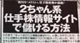 週刊SPA!7/24・31合併号のマネー(得)総本部のコーナーで当サイト『恐るべき注目銘柄株速報』のインタビュー記事が掲載されました。
===差が開いた ===
62 ID:0tI7dyqq
22 ID:W6VGvCEt
21 ID:V70C3the
20 ID:AeeNowQz
19 ID:gLd8KY7Y
15 ID:vH/j6VCc
14 ID:kdQUV6y/
14 ID:bSBoFbfD
14 ID:OH0p+TAc
14 ID:denTIfe3