shinseijapan

【恐るべき株】今急騰/急落している株、仕手株、低位株、思惑株、材料株など、今みんなが注目している銘柄をほぼリアルタイムでランキング化!個別株銘柄情報も口コミや掲示板など中心にまとめています。
【2ch】急騰株 急落株 仕手株 注目銘柄【Yahoo】ファイナンス掲示板(Y板)よりそれぞれの注目銘柄ランキングが表示され、 レス数ボタン・トピ数ボタンをクリックする事で最新銘柄口コミ情報が表示されます!気になる株式銘柄がある方は是非お試しください。 仕手・仕手株・仕手筋とは?

[お知らせ]
リアルタイム注目キーワードランキング をホームに設置しました。2ch市況1/株式板で今リアルタイムで話題の注目キーワードをご覧ください。 ※現在1位のキーワードは『オルツ』です
本日、仕手株として話題になっている銘柄は 仕手・仕手株 こちらの検索結果をご参考に。

【4335】アイ・ピー・エス【IPS】

1 : 管理人 : 2012/07/30(月) 20:30:38 ID:OwnerKabu685

アイ・ピー・エス[4335] - 独SAP社のERPパッケージ(統合業務ソフト、経営資源を管理、統合するシステム)「R/3」の導入サービスが中核。導入コンサルティングを行い、R/3の部品を組み合わせるとともに、部品がない業務機能は独自開発を行い、システムとしてパッケージ化。ERP市場は大手企業の導入が一巡、中堅・中小企業向けが中心に。中堅企業向けに求められる、高いコストパフォーマンスを追求。クラウド型サービスにも進出。

会社HP:ttp://www.ips.ne.jp/

前へ次へ

2 : 恐るべき山師さん : 2015/08/04(火) 23:29:48 ID:MDM4ZGI4ZmS8

  • good

    0
  • bad

    0
  • Re2

IPSをわたくし1200円で、大人買いしてます。今後どうですかね。

[4335]アイ・ピー・エス 2ch&Yahoo板統合 新着口コミ情報

※コメントは常に更新されます

【急騰】今買えばいい株22222【にゃんにゃん】 より

743 :山師さん:2025/04/24(木)10:38:29 ID:tZSUlLq1

4335IPS飛んだら同じ奴

Yahoo掲示板(Y板) - 4335より

497 :普段出来高が1万株も…:2025/04/22(火)19:01:00 ID:mas*****

普段出来高が1万株もない閑散株なのになんなんすかね インサイダーはここまで露骨にはやらないし

Yahoo掲示板(Y板) - 4335より

496 :いつものパターンね:2025/04/22(火)11:23:00 ID:wsw*****

いつものパターンね

【急騰】今買えばいい株22210【全無】 より

729 :山師さん:2025/04/22(火)11:22:16 ID:0KhRngjD

IPSオーバーキルおめw

Yahoo掲示板(Y板) - 4335より

495 :今日も、:2025/04/22(火)11:08:00 ID:wsw*****

今日も、やってはる☺️ 高値近辺で売り出しとく✌️

【急騰】今買えばいい株22210【全無】 より

598 :山師さん:2025/04/22(火)11:03:13 ID:v94CVOJk

アイ・ピー・エス

【急騰】今買えばいい株22210【全無】 より

593 :山師さん:2025/04/22(火)11:02:29 ID:0KhRngjD

IPS↑

【急騰】今買えばいい株22208【団鬼六】 より

536 :山師さん:2025/04/21(月)22:53:54 ID:fbXSdLse

Amid Trump’s tariffs, TSMC has been stepping up its investment in the U.S. According to Economic Daily News, the company is accelerating the timeline for its second Arizona fab. In addition, TSMC is reportedly set to introduce its latest fan-out panel-level packaging (FOPLP) technology in the U.S. to meet rising demand from customers seeking chips manufactured in the U.S.

The report highlights that, following major clients such as Apple, NVIDIA, and AMD announcing plans to expand their investments in the U.S., TSMC has accordingly adjusted its strategies.

TSMC is currently in its quiet period ahead of its earnings call and is unable to comment, as the report notes.

TSMC Advances FOPLP Technology

Citing Nikkei, the report states that TSMC is finalizing the specifications for its FOPLP technology in an effort to accelerate its mass production timeline. The first-generation version is expected to adopt a 300mm x 300mm panel size—smaller than the previously tested 510mm x 515mm format. According to the report, TSMC is currently building a pilot production line in Taoyuan, Taiwan, with limited trial production anticipated to begin as early as 2027.

The report also notes that TSMC initially explored partnering with panel makers such as Innolux but ultimately opted to develop the technology in-house, as the current precision and technical capabilities of the panel industry were deemed insufficient to meet TSMC’s standards.

As noted by the report, FOPLP offers improved heat dissipation compared to 3D stacking techniques such as wafer-on-wafer (WoW), CoWoS, and SoIC. However, its production efficiency is lower than that of existing 3D stacking methods. The report adds that AI customers are still expected to be the primary adopters of this packaging technology.

Tech Giants Fuel TSMC’s U.S. Manufacturing Expansion

Notably, on April 15, AMD CEO Lisa Su confirmed that the company is ramping up U.S. production. According to Reuters, AMD’s flagship chips will soon roll off TSMC’s new Arizona line—marking the first time its products will be manufactured in the U.S.

Meanwhile, NVIDIA recently also revealed plans to invest up to USD 500 billion in U.S.-based AI server production over the next four years and confirmed that its Blackwell chips are now being produced at TSMC’s Phoenix plant, as Reuters notes.

As noted by Economic Daily News, sources indicate that in response to requests from major clients such as AMD and Apple, TSMC has reportedly informed suppliers that equipment move-in for its second Arizona fab will begin as early as September this year—one full year ahead of schedule.

In other words, the fab’s 3nm production is now expected to begin by the end of 2027, while the second-phase line for 2nm is projected to enter mass production in 2028 as the report points out.

547 :山師さん:2025/04/21(月)23:01:35 Rfp0DKa2

>>536
荒らすなボケ!

【急騰】今買えばいい株22208【団鬼六】 より

528 :山師さん:2025/04/21(月)22:51:37 ID:HQwTJw7C

Amid Trump’s tariffs, TSMC has been stepping up its investment in the U.S. According to Economic Daily News, the company is accelerating the timeline for its second Arizona fab. In addition, TSMC is reportedly set to introduce its latest fan-out panel-level packaging (FOPLP) technology in the U.S. to meet rising demand from customers seeking chips manufactured in the U.S.

The report highlights that, following major clients such as Apple, NVIDIA, and AMD announcing plans to expand their investments in the U.S., TSMC has accordingly adjusted its strategies.

TSMC is currently in its quiet period ahead of its earnings call and is unable to comment, as the report notes.

TSMC Advances FOPLP Technology

Citing Nikkei, the report states that TSMC is finalizing the specifications for its FOPLP technology in an effort to accelerate its mass production timeline. The first-generation version is expected to adopt a 300mm x 300mm panel size—smaller than the previously tested 510mm x 515mm format. According to the report, TSMC is currently building a pilot production line in Taoyuan, Taiwan, with limited trial production anticipated to begin as early as 2027.

The report also notes that TSMC initially explored partnering with panel makers such as Innolux but ultimately opted to develop the technology in-house, as the current precision and technical capabilities of the panel industry were deemed insufficient to meet TSMC’s standards.

As noted by the report, FOPLP offers improved heat dissipation compared to 3D stacking techniques such as wafer-on-wafer (WoW), CoWoS, and SoIC. However, its production efficiency is lower than that of existing 3D stacking methods. The report adds that AI customers are still expected to be the primary adopters of this packaging technology.

Tech Giants Fuel TSMC’s U.S. Manufacturing Expansion

Notably, on April 15, AMD CEO Lisa Su confirmed that the company is ramping up U.S. production. According to Reuters, AMD’s flagship chips will soon roll off TSMC’s new Arizona line—marking the first time its products will be manufactured in the U.S.

Meanwhile, NVIDIA recently also revealed plans to invest up to USD 500 billion in U.S.-based AI server production over the next four years and confirmed that its Blackwell chips are now being produced at TSMC’s Phoenix plant, as Reuters notes.

As noted by Economic Daily News, sources indicate that in response to requests from major clients such as AMD and Apple, TSMC has reportedly informed suppliers that equipment move-in for its second Arizona fab will begin as early as September this year—one full year ahead of schedule.

In other words, the fab’s 3nm production is now expected to begin by the end of 2027, while the second-phase line for 2nm is projected to enter mass production in 2028 as the report points out.

【急騰】今買えばいい株22208【団鬼六】 より

527 :山師さん:2025/04/21(月)22:51:14 ID:N5bUdpKO

Amid Trump’s tariffs, TSMC has been stepping up its investment in the U.S. According to Economic Daily News, the company is accelerating the timeline for its second Arizona fab. In addition, TSMC is reportedly set to introduce its latest fan-out panel-level packaging (FOPLP) technology in the U.S. to meet rising demand from customers seeking chips manufactured in the U.S.

The report highlights that, following major clients such as Apple, NVIDIA, and AMD announcing plans to expand their investments in the U.S., TSMC has accordingly adjusted its strategies.

TSMC is currently in its quiet period ahead of its earnings call and is unable to comment, as the report notes.

TSMC Advances FOPLP Technology

Citing Nikkei, the report states that TSMC is finalizing the specifications for its FOPLP technology in an effort to accelerate its mass production timeline. The first-generation version is expected to adopt a 300mm x 300mm panel size—smaller than the previously tested 510mm x 515mm format. According to the report, TSMC is currently building a pilot production line in Taoyuan, Taiwan, with limited trial production anticipated to begin as early as 2027.

The report also notes that TSMC initially explored partnering with panel makers such as Innolux but ultimately opted to develop the technology in-house, as the current precision and technical capabilities of the panel industry were deemed insufficient to meet TSMC’s standards.

As noted by the report, FOPLP offers improved heat dissipation compared to 3D stacking techniques such as wafer-on-wafer (WoW), CoWoS, and SoIC. However, its production efficiency is lower than that of existing 3D stacking methods. The report adds that AI customers are still expected to be the primary adopters of this packaging technology.

Tech Giants Fuel TSMC’s U.S. Manufacturing Expansion

Notably, on April 15, AMD CEO Lisa Su confirmed that the company is ramping up U.S. production. According to Reuters, AMD’s flagship chips will soon roll off TSMC’s new Arizona line—marking the first time its products will be manufactured in the U.S.

Meanwhile, NVIDIA recently also revealed plans to invest up to USD 500 billion in U.S.-based AI server production over the next four years and confirmed that its Blackwell chips are now being produced at TSMC’s Phoenix plant, as Reuters notes.

As noted by Economic Daily News, sources indicate that in response to requests from major clients such as AMD and Apple, TSMC has reportedly informed suppliers that equipment move-in for its second Arizona fab will begin as early as September this year—one full year ahead of schedule.

In other words, the fab’s 3nm production is now expected to begin by the end of 2027, while the second-phase line for 2nm is projected to enter mass production in 2028 as the report points out.

【急騰】今買えばいい株22208【団鬼六】 より

526 :山師さん:2025/04/21(月)22:51:03 ID:+p5wlGn+

Amid Trump’s tariffs, TSMC has been stepping up its investment in the U.S. According to Economic Daily News, the company is accelerating the timeline for its second Arizona fab. In addition, TSMC is reportedly set to introduce its latest fan-out panel-level packaging (FOPLP) technology in the U.S. to meet rising demand from customers seeking chips manufactured in the U.S.

The report highlights that, following major clients such as Apple, NVIDIA, and AMD announcing plans to expand their investments in the U.S., TSMC has accordingly adjusted its strategies.

TSMC is currently in its quiet period ahead of its earnings call and is unable to comment, as the report notes.

TSMC Advances FOPLP Technology

Citing Nikkei, the report states that TSMC is finalizing the specifications for its FOPLP technology in an effort to accelerate its mass production timeline. The first-generation version is expected to adopt a 300mm x 300mm panel size—smaller than the previously tested 510mm x 515mm format. According to the report, TSMC is currently building a pilot production line in Taoyuan, Taiwan, with limited trial production anticipated to begin as early as 2027.

The report also notes that TSMC initially explored partnering with panel makers such as Innolux but ultimately opted to develop the technology in-house, as the current precision and technical capabilities of the panel industry were deemed insufficient to meet TSMC’s standards.

As noted by the report, FOPLP offers improved heat dissipation compared to 3D stacking techniques such as wafer-on-wafer (WoW), CoWoS, and SoIC. However, its production efficiency is lower than that of existing 3D stacking methods. The report adds that AI customers are still expected to be the primary adopters of this packaging technology.

Tech Giants Fuel TSMC’s U.S. Manufacturing Expansion

Notably, on April 15, AMD CEO Lisa Su confirmed that the company is ramping up U.S. production. According to Reuters, AMD’s flagship chips will soon roll off TSMC’s new Arizona line—marking the first time its products will be manufactured in the U.S.

Meanwhile, NVIDIA recently also revealed plans to invest up to USD 500 billion in U.S.-based AI server production over the next four years and confirmed that its Blackwell chips are now being produced at TSMC’s Phoenix plant, as Reuters notes.

As noted by Economic Daily News, sources indicate that in response to requests from major clients such as AMD and Apple, TSMC has reportedly informed suppliers that equipment move-in for its second Arizona fab will begin as early as September this year—one full year ahead of schedule.

In other words, the fab’s 3nm production is now expected to begin by the end of 2027, while the second-phase line for 2nm is projected to enter mass production in 2028 as the report points out.

【急騰】今買えばいい株22208【団鬼六】 より

521 :山師さん:2025/04/21(月)22:50:11 ID:rwHZuuRz

Amid Trump’s tariffs, TSMC has been stepping up its investment in the U.S. According to Economic Daily News, the company is accelerating the timeline for its second Arizona fab. In addition, TSMC is reportedly set to introduce its latest fan-out panel-level packaging (FOPLP) technology in the U.S. to meet rising demand from customers seeking chips manufactured in the U.S.

The report highlights that, following major clients such as Apple, NVIDIA, and AMD announcing plans to expand their investments in the U.S., TSMC has accordingly adjusted its strategies.

TSMC is currently in its quiet period ahead of its earnings call and is unable to comment, as the report notes.

TSMC Advances FOPLP Technology

Citing Nikkei, the report states that TSMC is finalizing the specifications for its FOPLP technology in an effort to accelerate its mass production timeline. The first-generation version is expected to adopt a 300mm x 300mm panel size—smaller than the previously tested 510mm x 515mm format. According to the report, TSMC is currently building a pilot production line in Taoyuan, Taiwan, with limited trial production anticipated to begin as early as 2027.

The report also notes that TSMC initially explored partnering with panel makers such as Innolux but ultimately opted to develop the technology in-house, as the current precision and technical capabilities of the panel industry were deemed insufficient to meet TSMC’s standards.

As noted by the report, FOPLP offers improved heat dissipation compared to 3D stacking techniques such as wafer-on-wafer (WoW), CoWoS, and SoIC. However, its production efficiency is lower than that of existing 3D stacking methods. The report adds that AI customers are still expected to be the primary adopters of this packaging technology.

Tech Giants Fuel TSMC’s U.S. Manufacturing Expansion

Notably, on April 15, AMD CEO Lisa Su confirmed that the company is ramping up U.S. production. According to Reuters, AMD’s flagship chips will soon roll off TSMC’s new Arizona line—marking the first time its products will be manufactured in the U.S.

Meanwhile, NVIDIA recently also revealed plans to invest up to USD 500 billion in U.S.-based AI server production over the next four years and confirmed that its Blackwell chips are now being produced at TSMC’s Phoenix plant, as Reuters notes.

As noted by Economic Daily News, sources indicate that in response to requests from major clients such as AMD and Apple, TSMC has reportedly informed suppliers that equipment move-in for its second Arizona fab will begin as early as September this year—one full year ahead of schedule.

In other words, the fab’s 3nm production is now expected to begin by the end of 2027, while the second-phase line for 2nm is projected to enter mass production in 2028 as the report points out.

【急騰】今買えばいい株22207【殺技団】 より

981 :山師さん:2025/04/21(月)18:01:28 ID:04LyRcZK

ドル円が後60pipsで140割れてしまうやん

【急騰】今買えばいい株22204【日本株暴騰】 より

142 :山師さん:2025/04/21(月)07:01:53 ID:Ad09o5Q+

住友ファーマどうすっかな
iPSはセルシードで製造に難があるってのがわかっているからクオリプスも下がったし創薬系の動きと違うんだよね

【急騰】今買えばいい株22201【ウジクロ】 より

380 :山師さん:2025/04/18(金)17:38:39 ID:JuLY+Rg8

ips系元気やな

【急騰】今買えばいい株22199【週末どこ行こ】 より

70 :山師さん:2025/04/18(金)10:42:12 ID:VA4P111J

iPSとかだいたい新技術とかは10年後に花開くからなAIも話題になって10年だしそういう意味ではジオマテックのHRDPももうすぐ実を結ぶときなんだよね
次世代半導体のデファクトスタンダードになれれば莫大な利益が今後しばらくもたらされる事になる

【急騰】今買えばいい株22197【コロコロ恫喝】 より

841 :山師さん:2025/04/18(金)08:17:26 ID:sx6I82Ml

iPSといえばクオリプスの値動き怖えよ

【急騰】今買えばいい株22197【コロコロ恫喝】 より

832 :山師さん:2025/04/18(金)08:10:23 ID:qQl1iSUZ

IPS関連と言えば4390来るか?

【急騰】今買えばいい株22197【コロコロ恫喝】 より

829 :山師さん:2025/04/18(金)08:09:35 ID:6d1oGGQA

IPS関連が動いているから調整十分なクオリプスいいな
7000円を底にしてるから低リスクだし惚れてしまう

Yahoo掲示板(Y板) - 4335より

494 :もうちょい取れたけど…:2025/04/17(木)17:54:00 ID:toj

もうちょい取れたけど、抜けれたからいいや

Yahoo掲示板(Y板) - 4335より

493 :打ち上げ花火のような…:2025/04/17(木)14:50:00 ID:Mar

打ち上げ花火のような値動きだったね。 自分はまだまだ塩漬け。

Yahoo掲示板(Y板) - 4335より

492 :ま~た荒らしか。:2025/04/17(木)14:47:00 ID:猫ちゃうまん。(TecHunt)

ま~た荒らしか。 最近毎日グロース同じ動きする銘柄多数

Yahoo掲示板(Y板) - 4335より

491 :あーあw:2025/04/17(木)14:22:00 ID:ごろう

あーあw

Yahoo掲示板(Y板) - 4335より

490 :どうしたの?:2025/04/17(木)14:16:00 ID:どんどこどん

どうしたの?

Yahoo掲示板(Y板) - 4335より

489 :しまった!!見逃した…:2025/04/17(木)14:13:00 ID:wsw*****

しまった!!見逃した(´;ω;`)

【急騰】今買えばいい株22195【金持ち喧嘩せず】 より

437 :山師さん:2025/04/17(木)14:09:14 ID:2rtRM6qX

アイピーエスにぶんなげきたー

続きは4335銘柄情報ページでご確認ください

前へ次へ

掲示板書き込み

  • スパム対策の為、URLは"h"を抜いた"ttp"から入力して下さい。
  • 宣伝目的と思われる書き込みに記載されたURLにはサイト内銘柄ページ、ブログランキング他、当サイトからのリンクを全て除外させて頂きます。
お名前: 銘柄コード: 削除キー

規約に同意する。

banner

wait
  • 株式投資 - みんなのお金儲けアンテナ[ブログランキング]
  • 投資ギャンブル ブログサイトランキング
  • 株ライン~ツイッターで株式銘柄探し 株価情報~

2ch市況1/株式板 話題ランキング

2chの急騰急落銘柄/今買えばいい株スレ等でのレス数ランキング(過去3日)

市況1板勢いランキング

2ch市況1板内に専用スレのある株式銘柄のランキング。レスの勢いがある銘柄順に並び替えています。
(参考:2ちゃんねる全板・勢いランキング

ランク 銘柄 Pt
1 4565 ネクセラファーマ(株) 13

株式銘柄 関連銘柄別2chレス数ランキング

株式銘柄 関連銘柄別yahooトピ数ランキング

株式銘柄 業種別2chレス数ランキング

株式銘柄 業種別yahooトピ数ランキング

当サイトが週刊SPA!に掲載されました!

spa

2ちゃん系仕手株情報サイトで儲ける方法 
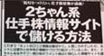
週刊SPA!7/24・31合併号のマネー(得)総本部のコーナーで当サイト『恐るべき注目銘柄株速報』のインタビュー記事が掲載されました。

週刊SPA!7/24・31合併号

blog_parts_sample

※このブログパーツは株ブログパーツページより無料配布中です

新着レス:

hide

top