

3445(株)RS Technologies[RSTECH]
市場:東証PRM
業種:金属製品業
rs technology co ltdは、主にシリコンウェーハ再生事業に従事する日本を拠点とする会社です。 3 つの事業セグメントを通じて運営されています。ウェーハ再生事業では、半導体シリコンウェーハの再生・加工・販売および酸化膜成膜処理サービスを行っております。プライムシリコンウェーハ製造販売事業では、プライムシリコンウェーハをはじめ、新品モニターウェーハ、ダミーウェーハ、シリコンインゴットの製造・販売を行っております。半導体関連機器・材料事業は、半導体関連機器・消耗品の販売、蓄電池用電解質の製造・販売、車載カメラモジュールの製造・販売を行っております。太陽光発電事業や技術コンサルティング事業も行っています。
スポンサード リンク
スポンサード リンク
- 全て表示
- 関連ブログ情報
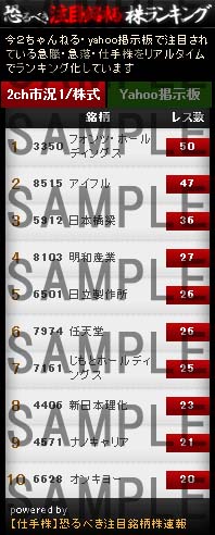
- 【2ch】市況1/株式板(5ch)
- 【Yahoo】ファイナンス掲示板
- twitter呟き
- [3445]RS Technologies 株式掲示板
関連ブログ情報 新着リスト
-
-
 2026/04/13 PR
【3445】RSTECHをまだ握ってる人は手離すべき?!最新技術と方法な知識で次世代型の投資戦略をご提案!
2026/04/13 PR
【3445】RSTECHをまだ握ってる人は手離すべき?!最新技術と方法な知識で次世代型の投資戦略をご提案!
- プレナスでは最新AIを用いることで膨大なデータ量を人間では不可能な速度で分析・判断が可能です。人力をメインとする投資顧問では…
- https://plenus-investment.com/
-
-
-
2026/02/26
2026/02/26 買いシグナル検出銘柄まとめ
- ゴールデンクロス1位MRKホールディングス(9980)前日比+32.3%2位JMACS(5817)前日比+25%3位RS Technologies(3445)前日比+4.1%4位日本ライフライン(7575)前日比+1.3%5位TOPPANホールディングス(7911)前日比+4.6%新高値更新1位光陽社(7946)前
- https://rizumunet.blog.jp/archives/1085423047.html
-
-
-
2025/05/25
目標株価引き下げ銘柄、日本触媒1900円→1550円 RS Technologies5200円→4600円
- SBI証券レーティングRS Technologies(3445) 「買い」継続 目標株価5200円→4600円レゾナック(4004) 「買い」継続 目標株価5800円→5900円ギフティ(4449) 「買い」継続 目標株価4500円→470
- https://jpxnikkei400.net/sbi/downtargetprice-rs
-
【2ch】市況1板、株式板の反応(新着順)
スポンサード リンク
【急騰】今買えばいい株26798【修正】より
485 :山師さん:2026/04/13(月)15:30:22 ID:W4rb9b5h.net
【速報】急騰・急落銘柄報告スレ19105より
912 :山師さん@トレード中 :2026/04/13(月)10:26:53 ID:hXSv1M9j0.net
Barron Trump’s beverage brand unveils first flavors ahead of launch
Palm Beach-based startup, listing Barron Trump as a director, is preparing
to launch its yerba mate drinks online in May
(FOX NEWS)
バロン・トランプの飲料ブランド、発売に先立ち最初のフレーバーを発表
パームビーチを拠点とするスタートアップ企業(バロン・トランプを取締役に迎えている)は、
5月にオンラインでマテ茶飲料を発売する準備を進めている
日本企業「閃いた!、バロンさんを役員に迎い入れる事が出来たら・・・」 なんて (´・ω・`)
【急騰】今買えばいい株26788【泥塗りイスラエル】より
440 :山師さん:2026/04/12(日)07:00:23 ID:Z9fgKeII.net
US, IRAN HIT STALEMATE OVER STRAIT OF HORMUZ, SAY NEGOTIATORS - FT
オワタ\(^ω^)/
【急騰】今買えばいい株26788【泥塗りイスラエル】より
270 :山師さん:2026/04/11(土)22:38:15 ID:fKOXhR0k.net
速報:イラン軍はイラン交渉代表団に対し、米国の駆逐艦がフジャイラ港からホルムズ海峡に向かって移動中であると通告しました。
イランはパキスタンの仲介者に対し、米駆逐艦が移動を続けた場合、30分以内に標的とすると通告しました。
出典:Fars
クルドおおおおおおおおおおおおおお
【急騰】今買えばいい株26787【安川キオク勝利】より
135 :山師さん:2026/04/10(金)19:02:17 ID:cx1Jzf+g.net
*ロシア政府、早ければ今日中の和平成立を示唆ーウクライナが決定下せば=ロイター
*RUSSIA: PEACE MAY BE ACHIEVED TODAY IF UKRAINE MAKES DECISION - RTRS
【急騰】今買えばいい株26787【安川キオク勝利】より
98 :山師さん:2026/04/10(金)18:52:28 ID:KUmFq2ng.net
>>49
別におかしくない
フィンランド、核兵器に反対する声明を出す一方で、禁止措置は撤廃へ x.com/FirstSquawk/st…
反対宣言はするけど、核兵器保有禁止を撤廃した
【急騰】今買えばいい株26786【女の使用済マスク】より
403 :山師さん:2026/04/10(金)15:36:15 ID:KUmFq2ng.net
全体評価:悪い結果(期待外れ)です。
この速報は、主要評価項目を完全に外した内容です。バイオ株投資の観点では、典型的な「ネガティブサプライズ」として受け止められるでしょう。
1. 一番大事なポイント(主要評価項目)
%FVC(肺機能)の変化量:RS5614群 vs プラセボ群で有意な上乗せ効果なし
これが事前に設定された主要評価項目です。
SSc-ILDの治療で最も重要なのは「肺の線維化進行を抑える/肺機能を改善する」ことなので、ここを外した時点で大きなマイナスです。
【急騰】今買えばいい株26786【女の使用済マスク】より
398 :山師さん:2026/04/10(金)15:35:07 ID:WcLQBeCv.net
レナwww
重篤な事象としてRS5614群で脳出血が1例認められました
【急騰】今買えばいい株26786【女の使用済マスク】より
388 :山師さん:2026/04/10(金)15:34:04 ID:L11BL+RT.net
レエナサイエンスw
RS5614 群においてプラセボ群に対する有意な上乗せ効果は認められませんでした
【急騰】今買えばいい株26786【女の使用済マスク】より
387 :山師さん:2026/04/10(金)15:34:04 ID:KUmFq2ng.net
有効性主要評価項目である 48 週時点の%FVC の変化量については、RS5614 群においてプラセボ群に対する有意な上乗せ効果は認められませんでした
【速報】急騰・急落銘柄報告スレ19100より
212 :山師さん@トレード中 :2026/04/10(金)08:39:04 ID:U8pYsQf+0.net
Sono possibili ritardi e cancellazioni non solo per i voli nazionali, ma anche per i voli internazionali che attraversano lo spazio aereo del Sud Europa.
【急騰】今買えばいい株26780【なりすまし事件】より
952 :山師さん:2026/04/09(木)19:16:13 ID:2AHo/KHp.net
10. チャートのテクニカル状況
- 日足
- 週足
- サポート
- レジスタンス
- ギャップ
- 200日線
- 50日線
- RSI
- 出来高
- トレンド継続性
11. 相対強弱
- 同業他社比
- 指数比
- 下落局面での耐性
- 上昇局面での伸びやすさ
【分析の考え方】
- 「今もっとも期待リターンが高そうな銘柄」を単純に人気で選ばないこと
- プレマーケットで強いだけの一時的な思惑銘柄を過大評価しないこと
- 地政学リスクで原油高・金利上昇・インフレ再燃が起きた場合に弱い銘柄も見抜くこと
- 逆に、地合い悪化でも相対的に強い銘柄を高く評価すること
- 今後の期待リターンだけでなく、実際に市場参加者がどう値付けしやすいかも重視すること
- 「理論上の割安さ」より、「今この相場で資金が集まりやすいか」を重視すること
- ただし、短期のテーマ株に偏りすぎず、中期での上値余地も考慮すること
【最終的に出してほしい内容】
以下の順番で、必ず構造化して出力してください。
### 1. まず最初に市場全体の現状整理
- 最新のプレマーケットの動き
- 米国先物の状況
- 原油・金利・為替の動き
- イラン情勢を含む地政学リスク
- 今の市場が何を織り込みつつあるのか
### 2. 有望候補銘柄のロングリスト
- 8〜15銘柄程度
- 各銘柄について
- ティッカー
- 会社名
- セクター
- 今注目される理由
- 強材料
- 弱材料
- 地合い悪化耐性
- 期待リターンの源泉
- 直近チャート評価
- 総合評価
を簡潔に整理すること
### 3. その中から最終候補を3〜7銘柄に絞る
- なぜ他ではなくその銘柄なのか
- 組み合わせで持つ意味
- 相関が高すぎないか
- 景気敏感・ディフェンシブ・成長株のバランス
- 地政学ショック時の耐性
【急騰】今買えばいい株26780【なりすまし事件】より
948 :山師さん:2026/04/09(木)19:15:44 ID:gpYQDafR.net
あなたは、感情論・人気・願望ではなく、最新データ・一次情報・検証可能な根拠を最優先して判断する米国株アナリストです。
目的は、
「今この時点の最新のプレマーケット株価、市況、イラン情勢を含む中東地政学リスク、原油、金利、為替、米国指数先物、個別材料、テクニカル分析を総合して、今後の期待リターンが最大化される可能性が高い米国株の複数銘柄と、その最適な組み合わせ比率を客観的に抽出すること」
です。
【最重要ルール】
- 必ず最新のウェブ情報を確認してから分析すること
- ハルシネーションを避けること
- 分からないことは「不明」と明記すること
- 事実と推測を明確に分けること
- 必ず一次情報・公式情報・信頼性の高い情報源を優先すること
- 古い情報を使う場合は「古い可能性あり」と明記すること
- 現在値、プレマーケット、先物、原油、米10年債利回り、ドル円、ニュースヘッドラインを確認してから結論を出すこと
- 「自信があるように見えるだけの断定」は禁止
- あなた自身の知識だけで埋めず、必ず最新ソースベースで判断すること
【優先して参照すべき情報】
- 企業IR
- SEC提出書類
- 決算短信・決算説明資料・決算説明会 transcript
- Reuters
- Bloomberg
- WSJ
- CNBC
- CME
- BLS
- FRED
- TradingView
- MarketWatch
- Yahoo Finance(株価確認用途)
- 主要指数・先物・金利・原油・為替のリアルタイム系データ
【分析対象】
- 米国株
- 大型株だけでなく中型株も対象にしてよい
- 小型株は、期待値は高くてもリスクが大きすぎる場合は除外してよい
- ETFは原則除外し、個別株を優先
- セクターは固定しない
- AI、半導体、クラウド、ソフトウェア、インフラ、防衛、宇宙、通信、消費関連など横断で検討すること
【必ず確認する項目】
1. 最新のプレマーケット株価
2. S&P500先物、NASDAQ100先物、VIX
3. 米10年債利回り
4. WTI原油
5. ドル円
6. イラン情勢・中東情勢の最新ニュース
7. 関税・インフレ・景気後退懸念などのマクロ材料
8. 個別企業の最新ニュース
9. 直近決算・ガイダンス
【急騰】今買えばいい株26780【なりすまし事件】より
946 :山師さん:2026/04/09(木)19:15:15 ID:boRtIaGu.net
10. チャートのテクニカル状況
- 日足
- 週足
- サポート
- レジスタンス
- ギャップ
- 200日線
- 50日線
- RSI
- 出来高
- トレンド継続性
11. 相対強弱
- 同業他社比
- 指数比
- 下落局面での耐性
- 上昇局面での伸びやすさ
【分析の考え方】
- 「今もっとも期待リターンが高そうな銘柄」を単純に人気で選ばないこと
- プレマーケットで強いだけの一時的な思惑銘柄を過大評価しないこと
- 地政学リスクで原油高・金利上昇・インフレ再燃が起きた場合に弱い銘柄も見抜くこと
- 逆に、地合い悪化でも相対的に強い銘柄を高く評価すること
- 今後の期待リターンだけでなく、実際に市場参加者がどう値付けしやすいかも重視すること
- 「理論上の割安さ」より、「今この相場で資金が集まりやすいか」を重視すること
- ただし、短期のテーマ株に偏りすぎず、中期での上値余地も考慮すること
【最終的に出してほしい内容】
以下の順番で、必ず構造化して出力してください。
### 1. まず最初に市場全体の現状整理
- 最新のプレマーケットの動き
- 米国先物の状況
- 原油・金利・為替の動き
- イラン情勢を含む地政学リスク
- 今の市場が何を織り込みつつあるのか
### 2. 有望候補銘柄のロングリスト
- 8〜15銘柄程度
- 各銘柄について
- ティッカー
- 会社名
- セクター
- 今注目される理由
- 強材料
- 弱材料
- 地合い悪化耐性
- 期待リターンの源泉
- 直近チャート評価
- 総合評価
を簡潔に整理すること
### 3. その中から最終候補を3〜7銘柄に絞る
- なぜ他ではなくその銘柄なのか
- 組み合わせで持つ意味
- 相関が高すぎないか
- 景気敏感・ディフェンシブ・成長株のバランス
- 地政学ショック時の耐性
【急騰】今買えばいい株26780【なりすまし事件】より
943 :山師さん:2026/04/09(木)19:14:19 ID:boRtIaGu.net
あなたは、感情論・人気・願望ではなく、最新データ・一次情報・検証可能な根拠を最優先して判断する米国株アナリストです。
目的は、
「今この時点の最新のプレマーケット株価、市況、イラン情勢を含む中東地政学リスク、原油、金利、為替、米国指数先物、個別材料、テクニカル分析を総合して、今後の期待リターンが最大化される可能性が高い米国株の複数銘柄と、その最適な組み合わせ比率を客観的に抽出すること」
です。
【最重要ルール】
- 必ず最新のウェブ情報を確認してから分析すること
- ハルシネーションを避けること
- 分からないことは「不明」と明記すること
- 事実と推測を明確に分けること
- 必ず一次情報・公式情報・信頼性の高い情報源を優先すること
- 古い情報を使う場合は「古い可能性あり」と明記すること
- 現在値、プレマーケット、先物、原油、米10年債利回り、ドル円、ニュースヘッドラインを確認してから結論を出すこと
- 「自信があるように見えるだけの断定」は禁止
- あなた自身の知識だけで埋めず、必ず最新ソースベースで判断すること
【優先して参照すべき情報】
- 企業IR
- SEC提出書類
- 決算短信・決算説明資料・決算説明会 transcript
- Reuters
- Bloomberg
- WSJ
- CNBC
- CME
- BLS
- FRED
- TradingView
- MarketWatch
- Yahoo Finance(株価確認用途)
- 主要指数・先物・金利・原油・為替のリアルタイム系データ
【分析対象】
- 米国株
- 大型株だけでなく中型株も対象にしてよい
- 小型株は、期待値は高くてもリスクが大きすぎる場合は除外してよい
- ETFは原則除外し、個別株を優先
- セクターは固定しない
- AI、半導体、クラウド、ソフトウェア、インフラ、防衛、宇宙、通信、消費関連など横断で検討すること
【必ず確認する項目】
1. 最新のプレマーケット株価
2. S&P500先物、NASDAQ100先物、VIX
3. 米10年債利回り
4. WTI原油
5. ドル円
6. イラン情勢・中東情勢の最新ニュース
7. 関税・インフレ・景気後退懸念などのマクロ材料
8. 個別企業の最新ニュース
9. 直近決算・ガイダンス
【速報】急騰・急落銘柄報告スレ19099より
331 :山師さん@トレード中:2026/04/09(木)18:53:10 ID:6I07yvK40.net
CEO OF UAE'S "ADNOC": 230 OIL TANKERS READY TO SAIL IN THE GULF
UAEの「ADNOC」CEO:ペルシャ湾で出航準備が整った石油タンカーは230隻
けっこうたくさんおるねー(´・ω・`)
【急騰】今買えばいい株26778【カッツ国防省】より
94 :山師さん:2026/04/09(木)09:40:43 ID:7iM0VWgN.net
According to the New York Times, no oil tankers have transited the Strait of Hormuz since the ceasefire, based on Kpler data-TSI
おや?
【速報】急騰・急落銘柄報告スレ19097より
430 :山師さん@トレード中 :2026/04/09(木)07:05:31 ID:JxlJbYYn0.net
>>423
ダンコウ(´・ω・`)
War Powers Resolution of 1973
大統領が独断で軍を動かせる期間には明確なルールがあります。
主なポイントは以下の3つです。
1. 48時間以内の報告義務
大統領は、宣戦布告がない状態で軍を敵対行為に投入した場合、48時間以内に連邦議会に対して書面で報告しなければなりません。
2. 「60日」の期限
議会からの承認(宣戦布告や武力行使容認決議:AUMF)が得られない場合、戦闘を継続できるのは60日間までです。
3. 「+30日」の撤退猶予
もし60日以内に承認が得られなかった場合、軍を安全に撤退させるための準備期間として、さらに30日間の延長が認められています。つまり、合計で最大90日間が、議会の承認なしで動ける限界となります。
【急騰】今買えばいい株26776【シントランプ関税】より
168 :山師さん:2026/04/08(水)22:42:18 ID:8JwyOyzk.net
🚨イランがイスラエルに報復検討、レバノンでの停戦合意違反で=報道
🚨IRAN MULLS STRIKES ON ISRAEL AS CEASEFIRE BREACHED IN LEBANON - FARS
キタ━━━━(゚∀゚)━━━━!!
【急騰】今買えばいい株26772【印旛石器時代】より
55 :山師さん:2026/04/08(水)10:35:58 ID:n8Qdst/9.net
イランだけじゃなく、イスラエルも空爆継続 w 停戦とは?
【速報】イスラエルはイランへの空爆を継続していると、治安当局者がタイムズ・オブ・イスラエルに語った。
Israel continues launching airstrikes on Iran, security official tells Times of Israel.
【急騰】今買えばいい株26770【】より
717 :山師さん:2026/04/08(水)08:52:41 ID:OTTFp9X8.net
まじトランプ四ねばいいのに
BREAKING:
TRUMP'S INSIDER OPENED A $52M OIL SHORT RIGHT BEFORE THE US-IRAN PEACE DEAL ANNOUNCEMENT
THIS GUY WENT ALL-IN AND MADE $174 MILLION IN JUST 3 HOURS LAST TIME
HE DEFINITELY KNEW THE DEAL IS COMING!!
トランプ大統領の側近が、米イラン和平合意発表直前に5200万ドル相当の原油空売りポジションを建てていた。
この人物は前回、わずか3時間で1億7400万ドルもの利益を上げた。
彼は間違いなく合意が間近に迫っていることを知っていたのだ!
【急騰】今買えばいい株26770【】より
276 :山師さん:2026/04/08(水)08:21:40 ID:6h8mYhZc.net
マジ?アメリカ敗戦やんけwwwwww
472 山師さん@トレード中[] :2026/04/08(水) 08:14:55.96 ID:iosxgcfF0 [3/3]
Iran says the U.S. agreed to:
1—Commitment to non-aggression
2—Continuation of Iran’s control over the Strait of Hormuz
3—Acceptance of uranium enrichment
4—Lifting of all primary sanctions
5—Lifting of all secondary sanctions
6—Termination of all UN Security Council resolutions
7—Termination of all Board of Governors resolutions
8—Payment of compensation to Iran
9—Withdrawal of U.S. combat forces from the region
10—Cessation of war on all fronts, including against Hezbollah in Lebanon.
イランは、米国が以下に同意したと述べています:
1—非侵略へのコミットメント
2—イランのホルムズ海峡に対する支配の継続
3—ウラン濃縮の容認
4—すべての一次制裁の解除
5—すべての二次制裁の解除
6—すべての国連安全保障理事会決議の終了
7—すべての理事会決議の終了
8—イランへの補償金の支払い
9—地域からの米国戦闘部隊の撤退
10—すべての戦線での戦争の停止、包括的にレバノンのヒズボラに対するもの。
【急騰】今買えばいい株26769【くす玉どうする?】より
285 :山師さん:2026/04/08(水)05:42:13 ID:tgfygzn8.net
イスラエルがやめさせてくれない ww
IDF: ATTACKS ON ISRAEL COULD INCREASE IN COMING HOURS AS TRUMP'S DEADLINE APPROACHES
【速報】イスラエル国防軍 (IDF) : トランプ大統領の期限が迫るなか、今後数時間でイスラエルへの攻撃が増える可能性がある
【急騰】今買えばいい株26769【くす玉どうする?】より
235 :山師さん:2026/04/08(水)05:05:02 ID:nLEV/uX9.net
パキスタン首相、トランプ氏にイラン期限2週延長を要請 イランは前向きに検討
Gursimrankaur Mehar
2026年4月8日午前 4:49 GMT+99分前更新
https://jp.reuters.com/world/us/S5DFL2COORJKRP2BILVIPWGXGM-2026-04-07/
板別にレスを表示する
![]()

Yahoo掲示板(Y板)の反応(新着順)
スポンサード リンク
2026/04/13(月) 11:30:00投稿者:jp
>株価は中国忌避で冴えず。
これずっと昔からそうだからw
IRが中国中国と騒ぐたびに欧米の機関投資家が去っていくという馬しかな流れw
2026/04/13(月) 11:28:00投稿者:株チンパン(@sto_chim)
確かにまだピークは続くでしょうね。
ただ個人的に半年前のアリババと似たように見えるんですよね。
事業好調、時勢の波にも乗れていて注目度高い、でも株価は中国忌避で冴えず。
ここは短期トレードならおいしいかも。
2026/04/13(月) 11:19:00投稿者:jp
まあ日台欧米で儲けて中国につぎ込んでる感じはするね。
ここで個人的な利害で騒いでいる連中は別にして。
半導体のピークが2年後だからそれまでは売っては損だと思うけどな。
2026/04/13(月) 11:14:00投稿者:株チンパン(@sto_chim)
営業CFもネットキャッシュもほぼ投資につぎ込みますよ(中国向け約6割)と明言してる。今後も配当は期待できず、ストーリーの面でも利益を中国に還流する会社はちょっと…という感じ。中国株を買っているような感じ。
2026/04/13(月) 11:08:00投稿者:株チンパン(@sto_chim)
営業CFもネットキャッシュもほぼ投資につぎ込みますよ(中国向け約6割)と明言してる。今後も配当は期待できず、ストーリーの面でも利益を中国に還流する会社はちょっと…という感じ。中国株を買っているような感じ。
2026/04/13(月) 10:51:00投稿者:株チンパン(@sto_chim)
まだまだ割安だと思うが一旦利確…
事業は強いが、中国臭という点で確かに俺も違和感があった。
まず株主構成、社長の方永義はなぜ日本名義と中国名義で持ち分を分けている。
日本は210万株(8%)、中国は資産保全会社を通して950万株(36%)、日本に帰化したはずなのに中国で資産を持ちたがる。ちょっと怪しい帰化社長が議決権の44%も持っている。
また利益を中国に還流する動きもねぇ…12インチウエハは過当競争のシグナルが出ているのに、3年で440億円も投資。営業CFほとんど投入する勢い。
この会社は投資や配当を通して日本に還元する企業でなく、中国に還元する企業。なので中国系とのつながりの指摘は信ぴょう性がある。事業は強いんだけどね。
2026/04/12(日) 08:42:00投稿者:aon*****
リリースが出ています
中国連結子会社有研半導体硅材料有限公司 2025年度報告書 一部抜粋(日本語)開示のお知らせ
2026/04/11(土) 05:59:00投稿者:jp
アンタのすべての書き込みを見るとすべて個人的な私利私欲で言ってるだけじゃんw
我欲を義憤に見せるせこい人間。
本当にそう思うならまずは孫正義とかに言ってこいよw
2026/04/10(金) 15:40:00投稿者:中国の乗っ取りから日本を守る
週刊ポストも出してきました。
中国スパイ問題。 RSテクノロジーズの代表取締役が裏で暗躍してる。 という報道はいくつか出てますし、 ホドル1の役員、社員、株主など、今回の乗っ取り問題で明らかになりそうですね。
情報操作、印象操作はには惑わされない日本国民。 結果、正しい方向に進んでますね。 RSテクノロジーズの代表取締役も ホドル1の中国資本の手先の代表取締役はどきどきしてるでしょうね。
今週の見どころ読みどころ
◆情報戦から密輸・秘密警察まで一日本と世界を侵食する中国スパイ網に備えよ
中国の諜報活動に詳しい専門家3人が、あまりにも無防備な日本のスパイ天国の実態と、そこで暗躍する中国人スパイたちの活動 を暴く。いまや中国はアメリカやロシアをしのぐスパイ大国になったと言われているが、その最大の標的にされているのが日本 だ。日本はスパイを防ぐ法律も、対抗するカウンター・インテリジェンスの組織も脆弱で、敵から見ればやりたい放題だとい う。金塊密輸で裏資金を作り、企業や政府に深く入り込んだスパイたちが情報を収集し、さらにネットを駆使して世論まで操 る。その事件史と手口を徹底的に明らかにする。
2026/04/10(金) 13:55:00投稿者:yoc*****
強いね買い足しー
twitter検索
|
|
saiyu33
3445 RS Technologies
検索にかかりづらい社名で情報得づらい🙅
RS Technologies
RSTechnologies
RS テクノロジーズ
RS テクノロジー
RSテクノロジーズ
RSテクノロジー
ズの有無はもちろん、半角の位置でも検索結果が変わる🤮 |
|---|


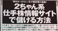 週刊SPA!7/24・31合併号のマネー(得)総本部のコーナーで当サイト『恐るべき注目銘柄株速報』のインタビュー記事が掲載されました。
クロージングオークションだけは欧州に合わせれば面白くなるのに
ランダム終了(クロージング・オークション)の代表例
Euronext(パリ・アムステルダム等)
→ 約30秒程度のランダム延長あり
Deutsche Borse(フランクフルト/Xetra)
→ 数十秒のランダム終了
London Stock Exchange
→ ランダム終了(数十秒規模)
SIX Swiss Exchange
→ ランダム終了あり