4335(株)アイピーエス[IPS]
市場:東証STD
業種:情報通信業
IPS Co。、Ltd。主に、エンタープライズリソースプランニング(ERP)のパッケージソフトウェアのインストールおよびメンテナンスビジネスに従事している日本を拠点とする企業です。 ERP用のパッケージソフトウェアは、販売、ロジスティクス、購買、コンピューターソフトウェアの機能への会計などのコアビジネス機能を統合することです。製品はSAP ERPです。実装サポートサービスは、特別なビジネス機能のための再建コンサルティングサービスの提供、およびSAP ERPの機能を完了するための実装開発エンジニアの提供に従事しています。メンテナンスサービスは、開発された周辺アプリケーションソフトウェアとインターフェースのメンテナンスと操作、機能的改善など、包括的なメンテナンス作業に従事しています。
関連: ソフト・システム開発/ERP/IT/RPA/EDI/Society5.0/人工知能/IoT/業務支援/働き方改革/デジタルトランスフォーメーション
スポンサード リンク
スポンサード リンク
- 全て表示
- 関連ブログ情報
- 【2ch】市況1/株式板(5ch)
- 【Yahoo】ファイナンス掲示板
- twitter呟き
- [4335]アイ・ピー・エス 株式掲示板
関連ブログ情報 新着リスト
-
-
2025/04/26 PR IPS(4335)を今から買って大丈夫か?不安要素はいくつかあります…。
- 株式投資の世界で勝ち続けるためには、「銘柄の選定」と「銘柄の売買タイミング」が大事です。適当な銘柄選定では勝てませんし、売買タイミングを誤ってしまうと…
- https://exiv.ne.jp/
-
-
-
2025/03/01 保有銘柄(2025年2月)
- 2月が終わりました。 毎月恒例の保有銘柄紹介です。 現金比率は49.0%から25.0%に下がりました。けっこう株を買いました。 月末の下げで、含み益を減らしました、、、。 <配当目的株> 40銘柄 1332ニッスイ、1605INPEX、1911住友林業、2428ウェルネット、2811カゴメ、2918わらべや日洋、3176三洋貿易、3355クリヤマHD、3569 セーレン、4204積水化学工業、4248竹本容器、4251恵和、4335アイ・ピー・エス、4486ユナイト&グロウ、4554富士製薬工業、4559ゼリア新薬工業、4972綜研化学、5334日本特殊陶業、5570ジェノバ、5713住友金属…
- https://richer-future.hatenablog.com/entry/2025/03/01/071403
-
-
-
2024/12/30 保有銘柄(2024年12月)
- 2024年の取引が終わりました。 日経平均は、わずかに4万円に届きませんでしたね。 さて、毎月恒例の、月末時点の保有銘柄を公開します。 現金比率は32.5%で、11月末から13%ほど引き上げました。 うち、「中小型成長株」部門は、現金比率を60%まで高めました。 三菱地所の株主通信(2025年3月期2Q) <配当株> 41銘柄 1605INPEX、177Aコージンバイオ、1911住友林業、2428ウェルネット、2811カゴメ、2918わらべや日洋、3191ジョイフル本田、3569 セーレン、4204積水化学工業、4206アイカ工業、4248竹本容器、4335アイ・ピー・エス、4554富士製薬工…
- https://richer-future.hatenablog.com/entry/2024/12/30/182320
-
-
-
2024/10/02 【159】アイ・ピー・エスさんから株主優待のクオ・カードが届きました
- クオカ、今年159社目で合計236,500円 アイ・ピー・エス(4335)さんから株主優待のクオ・カードが届きました 優待権利日 6月末日株価1026円、配…
- https://ameblo.jp/kabu1105/entry-12869696942.html
-
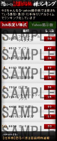
【2ch】市況1板、株式板の反応(新着順)
スポンサード リンク
【急騰】今買えばいい株22222【にゃんにゃん】 より
743 :山師さん:2025/04/24(木)10:38:29 ID:tZSUlLq1.net
【急騰】今買えばいい株22208【団鬼六】 より
536 :山師さん:2025/04/21(月)22:53:54 ID:fbXSdLse.net
Amid Trump’s tariffs, TSMC has been stepping up its investment in the U.S. According to Economic Daily News, the company is accelerating the timeline for its second Arizona fab. In addition, TSMC is reportedly set to introduce its latest fan-out panel-level packaging (FOPLP) technology in the U.S. to meet rising demand from customers seeking chips manufactured in the U.S.
The report highlights that, following major clients such as Apple, NVIDIA, and AMD announcing plans to expand their investments in the U.S., TSMC has accordingly adjusted its strategies.
TSMC is currently in its quiet period ahead of its earnings call and is unable to comment, as the report notes.
TSMC Advances FOPLP Technology
Citing Nikkei, the report states that TSMC is finalizing the specifications for its FOPLP technology in an effort to accelerate its mass production timeline. The first-generation version is expected to adopt a 300mm x 300mm panel size—smaller than the previously tested 510mm x 515mm format. According to the report, TSMC is currently building a pilot production line in Taoyuan, Taiwan, with limited trial production anticipated to begin as early as 2027.
The report also notes that TSMC initially explored partnering with panel makers such as Innolux but ultimately opted to develop the technology in-house, as the current precision and technical capabilities of the panel industry were deemed insufficient to meet TSMC’s standards.
As noted by the report, FOPLP offers improved heat dissipation compared to 3D stacking techniques such as wafer-on-wafer (WoW), CoWoS, and SoIC. However, its production efficiency is lower than that of existing 3D stacking methods. The report adds that AI customers are still expected to be the primary adopters of this packaging technology.
Tech Giants Fuel TSMC’s U.S. Manufacturing Expansion
Notably, on April 15, AMD CEO Lisa Su confirmed that the company is ramping up U.S. production. According to Reuters, AMD’s flagship chips will soon roll off TSMC’s new Arizona line—marking the first time its products will be manufactured in the U.S.
Meanwhile, NVIDIA recently also revealed plans to invest up to USD 500 billion in U.S.-based AI server production over the next four years and confirmed that its Blackwell chips are now being produced at TSMC’s Phoenix plant, as Reuters notes.
As noted by Economic Daily News, sources indicate that in response to requests from major clients such as AMD and Apple, TSMC has reportedly informed suppliers that equipment move-in for its second Arizona fab will begin as early as September this year—one full year ahead of schedule.
In other words, the fab’s 3nm production is now expected to begin by the end of 2027, while the second-phase line for 2nm is projected to enter mass production in 2028 as the report points out.
【急騰】今買えばいい株22208【団鬼六】 より
528 :山師さん:2025/04/21(月)22:51:37 ID:HQwTJw7C.net
Amid Trump’s tariffs, TSMC has been stepping up its investment in the U.S. According to Economic Daily News, the company is accelerating the timeline for its second Arizona fab. In addition, TSMC is reportedly set to introduce its latest fan-out panel-level packaging (FOPLP) technology in the U.S. to meet rising demand from customers seeking chips manufactured in the U.S.
The report highlights that, following major clients such as Apple, NVIDIA, and AMD announcing plans to expand their investments in the U.S., TSMC has accordingly adjusted its strategies.
TSMC is currently in its quiet period ahead of its earnings call and is unable to comment, as the report notes.
TSMC Advances FOPLP Technology
Citing Nikkei, the report states that TSMC is finalizing the specifications for its FOPLP technology in an effort to accelerate its mass production timeline. The first-generation version is expected to adopt a 300mm x 300mm panel size—smaller than the previously tested 510mm x 515mm format. According to the report, TSMC is currently building a pilot production line in Taoyuan, Taiwan, with limited trial production anticipated to begin as early as 2027.
The report also notes that TSMC initially explored partnering with panel makers such as Innolux but ultimately opted to develop the technology in-house, as the current precision and technical capabilities of the panel industry were deemed insufficient to meet TSMC’s standards.
As noted by the report, FOPLP offers improved heat dissipation compared to 3D stacking techniques such as wafer-on-wafer (WoW), CoWoS, and SoIC. However, its production efficiency is lower than that of existing 3D stacking methods. The report adds that AI customers are still expected to be the primary adopters of this packaging technology.
Tech Giants Fuel TSMC’s U.S. Manufacturing Expansion
Notably, on April 15, AMD CEO Lisa Su confirmed that the company is ramping up U.S. production. According to Reuters, AMD’s flagship chips will soon roll off TSMC’s new Arizona line—marking the first time its products will be manufactured in the U.S.
Meanwhile, NVIDIA recently also revealed plans to invest up to USD 500 billion in U.S.-based AI server production over the next four years and confirmed that its Blackwell chips are now being produced at TSMC’s Phoenix plant, as Reuters notes.
As noted by Economic Daily News, sources indicate that in response to requests from major clients such as AMD and Apple, TSMC has reportedly informed suppliers that equipment move-in for its second Arizona fab will begin as early as September this year—one full year ahead of schedule.
In other words, the fab’s 3nm production is now expected to begin by the end of 2027, while the second-phase line for 2nm is projected to enter mass production in 2028 as the report points out.
【急騰】今買えばいい株22208【団鬼六】 より
527 :山師さん:2025/04/21(月)22:51:14 ID:N5bUdpKO.net
Amid Trump’s tariffs, TSMC has been stepping up its investment in the U.S. According to Economic Daily News, the company is accelerating the timeline for its second Arizona fab. In addition, TSMC is reportedly set to introduce its latest fan-out panel-level packaging (FOPLP) technology in the U.S. to meet rising demand from customers seeking chips manufactured in the U.S.
The report highlights that, following major clients such as Apple, NVIDIA, and AMD announcing plans to expand their investments in the U.S., TSMC has accordingly adjusted its strategies.
TSMC is currently in its quiet period ahead of its earnings call and is unable to comment, as the report notes.
TSMC Advances FOPLP Technology
Citing Nikkei, the report states that TSMC is finalizing the specifications for its FOPLP technology in an effort to accelerate its mass production timeline. The first-generation version is expected to adopt a 300mm x 300mm panel size—smaller than the previously tested 510mm x 515mm format. According to the report, TSMC is currently building a pilot production line in Taoyuan, Taiwan, with limited trial production anticipated to begin as early as 2027.
The report also notes that TSMC initially explored partnering with panel makers such as Innolux but ultimately opted to develop the technology in-house, as the current precision and technical capabilities of the panel industry were deemed insufficient to meet TSMC’s standards.
As noted by the report, FOPLP offers improved heat dissipation compared to 3D stacking techniques such as wafer-on-wafer (WoW), CoWoS, and SoIC. However, its production efficiency is lower than that of existing 3D stacking methods. The report adds that AI customers are still expected to be the primary adopters of this packaging technology.
Tech Giants Fuel TSMC’s U.S. Manufacturing Expansion
Notably, on April 15, AMD CEO Lisa Su confirmed that the company is ramping up U.S. production. According to Reuters, AMD’s flagship chips will soon roll off TSMC’s new Arizona line—marking the first time its products will be manufactured in the U.S.
Meanwhile, NVIDIA recently also revealed plans to invest up to USD 500 billion in U.S.-based AI server production over the next four years and confirmed that its Blackwell chips are now being produced at TSMC’s Phoenix plant, as Reuters notes.
As noted by Economic Daily News, sources indicate that in response to requests from major clients such as AMD and Apple, TSMC has reportedly informed suppliers that equipment move-in for its second Arizona fab will begin as early as September this year—one full year ahead of schedule.
In other words, the fab’s 3nm production is now expected to begin by the end of 2027, while the second-phase line for 2nm is projected to enter mass production in 2028 as the report points out.
【急騰】今買えばいい株22208【団鬼六】 より
526 :山師さん:2025/04/21(月)22:51:03 ID:+p5wlGn+.net
Amid Trump’s tariffs, TSMC has been stepping up its investment in the U.S. According to Economic Daily News, the company is accelerating the timeline for its second Arizona fab. In addition, TSMC is reportedly set to introduce its latest fan-out panel-level packaging (FOPLP) technology in the U.S. to meet rising demand from customers seeking chips manufactured in the U.S.
The report highlights that, following major clients such as Apple, NVIDIA, and AMD announcing plans to expand their investments in the U.S., TSMC has accordingly adjusted its strategies.
TSMC is currently in its quiet period ahead of its earnings call and is unable to comment, as the report notes.
TSMC Advances FOPLP Technology
Citing Nikkei, the report states that TSMC is finalizing the specifications for its FOPLP technology in an effort to accelerate its mass production timeline. The first-generation version is expected to adopt a 300mm x 300mm panel size—smaller than the previously tested 510mm x 515mm format. According to the report, TSMC is currently building a pilot production line in Taoyuan, Taiwan, with limited trial production anticipated to begin as early as 2027.
The report also notes that TSMC initially explored partnering with panel makers such as Innolux but ultimately opted to develop the technology in-house, as the current precision and technical capabilities of the panel industry were deemed insufficient to meet TSMC’s standards.
As noted by the report, FOPLP offers improved heat dissipation compared to 3D stacking techniques such as wafer-on-wafer (WoW), CoWoS, and SoIC. However, its production efficiency is lower than that of existing 3D stacking methods. The report adds that AI customers are still expected to be the primary adopters of this packaging technology.
Tech Giants Fuel TSMC’s U.S. Manufacturing Expansion
Notably, on April 15, AMD CEO Lisa Su confirmed that the company is ramping up U.S. production. According to Reuters, AMD’s flagship chips will soon roll off TSMC’s new Arizona line—marking the first time its products will be manufactured in the U.S.
Meanwhile, NVIDIA recently also revealed plans to invest up to USD 500 billion in U.S.-based AI server production over the next four years and confirmed that its Blackwell chips are now being produced at TSMC’s Phoenix plant, as Reuters notes.
As noted by Economic Daily News, sources indicate that in response to requests from major clients such as AMD and Apple, TSMC has reportedly informed suppliers that equipment move-in for its second Arizona fab will begin as early as September this year—one full year ahead of schedule.
In other words, the fab’s 3nm production is now expected to begin by the end of 2027, while the second-phase line for 2nm is projected to enter mass production in 2028 as the report points out.
【急騰】今買えばいい株22208【団鬼六】 より
521 :山師さん:2025/04/21(月)22:50:11 ID:rwHZuuRz.net
Amid Trump’s tariffs, TSMC has been stepping up its investment in the U.S. According to Economic Daily News, the company is accelerating the timeline for its second Arizona fab. In addition, TSMC is reportedly set to introduce its latest fan-out panel-level packaging (FOPLP) technology in the U.S. to meet rising demand from customers seeking chips manufactured in the U.S.
The report highlights that, following major clients such as Apple, NVIDIA, and AMD announcing plans to expand their investments in the U.S., TSMC has accordingly adjusted its strategies.
TSMC is currently in its quiet period ahead of its earnings call and is unable to comment, as the report notes.
TSMC Advances FOPLP Technology
Citing Nikkei, the report states that TSMC is finalizing the specifications for its FOPLP technology in an effort to accelerate its mass production timeline. The first-generation version is expected to adopt a 300mm x 300mm panel size—smaller than the previously tested 510mm x 515mm format. According to the report, TSMC is currently building a pilot production line in Taoyuan, Taiwan, with limited trial production anticipated to begin as early as 2027.
The report also notes that TSMC initially explored partnering with panel makers such as Innolux but ultimately opted to develop the technology in-house, as the current precision and technical capabilities of the panel industry were deemed insufficient to meet TSMC’s standards.
As noted by the report, FOPLP offers improved heat dissipation compared to 3D stacking techniques such as wafer-on-wafer (WoW), CoWoS, and SoIC. However, its production efficiency is lower than that of existing 3D stacking methods. The report adds that AI customers are still expected to be the primary adopters of this packaging technology.
Tech Giants Fuel TSMC’s U.S. Manufacturing Expansion
Notably, on April 15, AMD CEO Lisa Su confirmed that the company is ramping up U.S. production. According to Reuters, AMD’s flagship chips will soon roll off TSMC’s new Arizona line—marking the first time its products will be manufactured in the U.S.
Meanwhile, NVIDIA recently also revealed plans to invest up to USD 500 billion in U.S.-based AI server production over the next four years and confirmed that its Blackwell chips are now being produced at TSMC’s Phoenix plant, as Reuters notes.
As noted by Economic Daily News, sources indicate that in response to requests from major clients such as AMD and Apple, TSMC has reportedly informed suppliers that equipment move-in for its second Arizona fab will begin as early as September this year—one full year ahead of schedule.
In other words, the fab’s 3nm production is now expected to begin by the end of 2027, while the second-phase line for 2nm is projected to enter mass production in 2028 as the report points out.
【急騰】今買えばいい株22204【日本株暴騰】 より
142 :山師さん:2025/04/21(月)07:01:53 ID:Ad09o5Q+.net
住友ファーマどうすっかな
iPSはセルシードで製造に難があるってのがわかっているからクオリプスも下がったし創薬系の動きと違うんだよね
【急騰】今買えばいい株22199【週末どこ行こ】 より
70 :山師さん:2025/04/18(金)10:42:12 ID:VA4P111J.net
iPSとかだいたい新技術とかは10年後に花開くからなAIも話題になって10年だしそういう意味ではジオマテックのHRDPももうすぐ実を結ぶときなんだよね
次世代半導体のデファクトスタンダードになれれば莫大な利益が今後しばらくもたらされる事になる
【急騰】今買えばいい株22198【鼻金】 より
719 :山師さん:2025/04/18(金)10:03:22 ID:kpQ4kknA.net
>>706
IPSから10年
それがいい結果になってきてるからね
嬉しいよ
【急騰】今買えばいい株22197【コロコロ恫喝】 より
829 :山師さん:2025/04/18(金)08:09:35 ID:6d1oGGQA.net
IPS関連が動いているから調整十分なクオリプスいいな
7000円を底にしてるから低リスクだし惚れてしまう
【急騰】今買えばいい株22195【金持ち喧嘩せず】 より
326 :山師さん:2025/04/17(木)14:00:14 ID:2rtRM6qX.net
アイピーエスは完全に見落としてた今日もくるとは
【急騰】今買えばいい株22195【金持ち喧嘩せず】 より
321 :山師さん:2025/04/17(木)13:59:52 ID:2rtRM6qX.net
山大もアイピーエスもきてるし雑技団まだ終わってないわ
【速報】急騰・急落銘柄報告スレ18258 より
194 :山師さん@トレード中 :2025/04/17(木)08:30:42 ID:Jc6NrJeC0.net
ファーマはIPS関連で上げてんね握ってた時もあったけどお薬株を長く持つのは怖すぎるんよー(´・ω・`)
【速報】急騰・急落銘柄報告スレ18251 より
332 :山師さん@トレード中:2025/04/14(月)22:17:25 ID:rkpB0GSn0.net
NVIDIA Blackwell chips have started production at TSMC's chip plants in Phoenix, Arizona.
エヌビディア・ブラックウェル・チップは、アリゾナ州フェニックスにあるTSMCのチップ工場で生産を開始した。
だそうです(´・ω・`)
【速報】急騰・急落銘柄報告スレ18247 より
573 :山師さん@トレード中 :2025/04/13(日)15:44:25 ID:gx1pQhaP0.net
Trump says he will provide more info on chips tariffs on Monday(ロイター)
トランプ大統領、月曜日にチップ関税の詳細情報を提供すると発表
https://www.reuters.com/world/us/trump-says-he-will-provide-more-info-chips-tariffs-monday-2025-04-13/
一応置いておきます
板別にレスを表示する
Yahoo掲示板(Y板)の反応(新着順)
スポンサード リンク
2025/04/22(火) 19:01:00投稿者:mas*****
普段出来高が1万株もない閑散株なのになんなんすかね
インサイダーはここまで露骨にはやらないし
2025/04/22(火) 11:23:00投稿者:wsw*****
いつものパターンね
2025/04/22(火) 11:08:00投稿者:wsw*****
今日も、やってはる☺️ 高値近辺で売り出しとく✌️
2025/04/17(木) 17:54:00投稿者:toj
もうちょい取れたけど、抜けれたからいいや
2025/04/17(木) 14:50:00投稿者:Mar
打ち上げ花火のような値動きだったね。
自分はまだまだ塩漬け。
2025/04/17(木) 14:47:00投稿者:猫ちゃうまん。(TecHunt)
ま~た荒らしか。
最近毎日グロース同じ動きする銘柄多数
2025/04/17(木) 14:22:00投稿者:ごろう
あーあw
2025/04/17(木) 14:16:00投稿者:どんどこどん
どうしたの?
2025/04/17(木) 14:13:00投稿者:wsw*****
しまった!!見逃した(´;ω;`)
2025/04/17(木) 13:57:00投稿者:ごろう
現場はここか
twitter検索
![]() |
kmttrade1
4335 アイ・ピー・エス
NKKスイッチズ、サステナブルな企業価値創造に向け、業務標準化と効率化の要となる基幹システムにGROW with SAPを採用
https://t.co/87qvIjj8OZ |
---|
![]() |
corp_newswatch
4335 アイ・ピー・エス 26.9億円
NKKスイッチズ、サステナブルな企業価値創造に向け、業務標準化と効率化の要となる基幹システムにGROW with SAPを採用
https://t.co/JnKm7cjD1I |
---|
![]() |
TigerstoSumo
4335アイ・ピー・エス、一時は300株で利益が15万ありましたが、いまは1500円😢株価の変動って凄いですね😭 |
---|
![]() |
irbank_of
4335 株式会社アイ・ピー・エス
自社株買い 上限:14万株、1億1000万円
(取得済)4万4100株、3301万円
取締役会(2023年1月6日)での決議状況(取得期間2023年2月10日~2023年6月30日)
https://t.co/M2QYrrUHhS |
---|
4335IPS飛んだら同じ奴