

DEVELOPの検索結果
2ch市況1板/株式板の今買えば良い株、Twitterの株アカ晒し、急騰・急落銘柄報告スレ、【下手】儲けられない人より集めたレスからの検索。過去一ヶ月前までのレスを表示します。
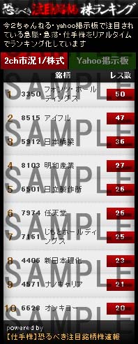
株/銘柄レス検索
「DEVELOP」のレス検索結果
検索結果5件 OR検索新着順
スポンサード リンク
521 :山師さん:2025/04/21(月) 22:50:11 ID:rwHZuuRz 【急騰】今買えばいい株22208【団鬼六】 より
788 :山師さん:2025/04/10(木) 00:20:19 ID:R7wYE3t+ 【急騰】今買えばいい株22156【世界変革の時】 より
SCOOP: People close to the Trump White House say you can expect an announcement of some sort about formal negotiations over trade and tariffs with Japan, Vietnam, and possibly the UK as early as today. Im not sure how much this moves the needle if it does go down (I always hedge w Trump who is unpredictable and these are inherently unpredictable times). Japan and Vietnam were already moving in this direction; UK is a long-time trading partner. But it's better than the alternative. And it does change the market narrative of doom and gloom. Story developing
スポンサード リンク
スポンサード リンク


 週刊SPA!7/24・31合併号のマネー(得)総本部のコーナーで当サイト『恐るべき注目銘柄株速報』のインタビュー記事が掲載されました。
Amid Trump’s tariffs, TSMC has been stepping up its investment in the U.S. According to Economic Daily News, the company is accelerating the timeline for its second Arizona fab. In addition, TSMC is reportedly set to introduce its latest fan-out panel-level packaging (FOPLP) technology in the U.S. to meet rising demand from customers seeking chips manufactured in the U.S.
The report highlights that, following major clients such as Apple, NVIDIA, and AMD announcing plans to expand their investments in the U.S., TSMC has accordingly adjusted its strategies.
TSMC is currently in its quiet period ahead of its earnings call and is unable to comment, as the report notes.
TSMC Advances FOPLP Technology
Citing Nikkei, the report states that TSMC is finalizing the specifications for its FOPLP technology in an effort to accelerate its mass production timeline. The first-generation version is expected to adopt a 300mm x 300mm panel size—smaller than the previously tested 510mm x 515mm format. According to the report, TSMC is currently building a pilot production line in Taoyuan, Taiwan, with limited trial production anticipated to begin as early as 2027.
The report also notes that TSMC initially explored partnering with panel makers such as Innolux but ultimately opted to develop the technology in-house, as the current precision and technical capabilities of the panel industry were deemed insufficient to meet TSMC’s standards.
As noted by the report, FOPLP offers improved heat dissipation compared to 3D stacking techniques such as wafer-on-wafer (WoW), CoWoS, and SoIC. However, its production efficiency is lower than that of existing 3D stacking methods. The report adds that AI customers are still expected to be the primary adopters of this packaging technology.
Tech Giants Fuel TSMC’s U.S. Manufacturing Expansion
Notably, on April 15, AMD CEO Lisa Su confirmed that the company is ramping up U.S. production. According to Reuters, AMD’s flagship chips will soon roll off TSMC’s new Arizona line—marking the first time its products will be manufactured in the U.S.
Meanwhile, NVIDIA recently also revealed plans to invest up to USD 500 billion in U.S.-based AI server production over the next four years and confirmed that its Blackwell chips are now being produced at TSMC’s Phoenix plant, as Reuters notes.
As noted by Economic Daily News, sources indicate that in response to requests from major clients such as AMD and Apple, TSMC has reportedly informed suppliers that equipment move-in for its second Arizona fab will begin as early as September this year—one full year ahead of schedule.
In other words, the fab’s 3nm production is now expected to begin by the end of 2027, while the second-phase line for 2nm is projected to enter mass production in 2028 as the report points out.