plenus

【恐るべき株】今急騰/急落している株、仕手株、低位株、思惑株、材料株など、今みんなが注目している銘柄をほぼリアルタイムでランキング化!個別株銘柄情報も口コミや掲示板など中心にまとめています。
【2ch】急騰株 急落株 仕手株 注目銘柄【Yahoo】ファイナンス掲示板(Y板)よりそれぞれの注目銘柄ランキングが表示され、 レス数ボタン・トピ数ボタンをクリックする事で最新銘柄口コミ情報が表示されます!気になる株式銘柄がある方は是非お試しください。 仕手・仕手株・仕手筋とは?

[お知らせ]
リアルタイム注目キーワードランキング をホームに設置しました。2ch市況1/株式板で今リアルタイムで話題の注目キーワードをご覧ください。 ※現在1位のキーワードは『トランプ』です
本日、仕手株として話題になっている銘柄は 仕手・仕手株 こちらの検索結果をご参考に。

【300】MIC【300】

1 : 管理人 : 2025/03/21(金) 06:50:16 ID:OwnerKabu685

MIC[300] - ドラッグストアや日用品メーカーなどに向け販促支援を提供。販促物の共同配送サービスも


前へ次へ

現在書き込みはありません。
MICを保有している方や思惑のある方は、ぜひ書き込みして行ってください!

MICの銘柄情報はコチラ→300

[300]MIC 2ch&Yahoo板統合 新着口コミ情報

※コメントは常に更新されます

Yahoo掲示板(Y板) - 300より

244 :予測:2025/05/07(水)13:12:00 ID:a65*****

予測

Yahoo掲示板(Y板) - 300より

243 :(続き)利益面に関し…:2025/05/06(火)20:41:00 ID:肉

(続き) 利益面に関して、私たちの収益力は10パーセントから17パーセントという実績があります。上場に向けた準備の中で一時的に投資へのアクセルを踏んだところもありましたが、利益率を10パーセント、さらにはその先に戻していくことが今後の計画になります。 したがって、来期は売上10パーセント前後、経常利益率10パーセント前後の成長をイメージしています。詳細な数字が出ましたら、あらためて発表します。 私たちの基本的な計画としては、毎年10パーセントから15パーセントの売上成長を維持すること、収益力についても10パーセントから15パーセントの利益を出していくことです。 決算説明動画の説明すね。 >『来期は売上10パーセント前後、経常利益率10パーセント前後の成長をイメージしています。』って言ってたから、来期の営利、純利は昨対比どんくらいになるか計算してみましょう

Yahoo掲示板(Y板) - 300より

242 :『来期は売上10パー…:2025/05/06(火)20:39:00 ID:肉

『来期は売上10パーセント前後、経常利益率10パーセント前後の成長をイメージしています。』って言ってたから、来期の営利、純利は昨対比どんくらいになるか計算してみましょう

Yahoo掲示板(Y板) - 300より

241 :決算説明動画で毎期1…:2025/05/04(日)22:17:00 ID:HAKU

決算説明動画で毎期10%~15%の成長率って この価格からやったら売られるでしょ(;^ω^)

Yahoo掲示板(Y板) - 300より

240 :ここはもう一段階上が…:2025/05/01(木)22:00:00 ID:eb1*****

ここはもう一段階上がると思ってますが、どうなりますかね〜。

【速報】急騰・急落銘柄報告スレ18287 より

232 :山師さん@トレード中 :2025/04/30(水)17:58:32 ID:LZaG69/30

Pres Xi: China Needs To Adapt To Changing Situations - Xinhua
- China To Adjust Economic Plan Based On Global Change
- To Promote Transformation Of Traditional Industries
- Urges Measures To Stabilize Employment
- Stabilize Markets And Expectations
習主席:中国は状況の変化に適応する必要がある-新華社
-中国、世界の変化に基づき経済計画を調整へ
-伝統産業の転換を推進へ
-雇用安定に向けた措置を促す
-市場と期待の安定化

普通やないかい(´・ω・`)

Yahoo掲示板(Y板) - 300より

238 :回戻す❌ 買い戻す⭕…:2025/04/30(水)11:40:00 ID:a65*****

回戻す❌ 買い戻す⭕️ ご無礼。

Yahoo掲示板(Y板) - 300より

237 :5.14前に仕込むか…:2025/04/30(水)11:38:00 ID:a65*****

5.14前に仕込むか!  5.7売りで 5.13回戻すか 迷ってる

【速報】急騰・急落銘柄報告スレ18282 より

516 :山師さん@トレード中 :2025/04/28(月)15:56:47 ID:mx9qeIQg0

After Abenomics

【急騰】今買えばいい株22208【団鬼六】 より

536 :山師さん:2025/04/21(月)22:53:54 ID:fbXSdLse

Amid Trump’s tariffs, TSMC has been stepping up its investment in the U.S. According to Economic Daily News, the company is accelerating the timeline for its second Arizona fab. In addition, TSMC is reportedly set to introduce its latest fan-out panel-level packaging (FOPLP) technology in the U.S. to meet rising demand from customers seeking chips manufactured in the U.S.

The report highlights that, following major clients such as Apple, NVIDIA, and AMD announcing plans to expand their investments in the U.S., TSMC has accordingly adjusted its strategies.

TSMC is currently in its quiet period ahead of its earnings call and is unable to comment, as the report notes.

TSMC Advances FOPLP Technology

Citing Nikkei, the report states that TSMC is finalizing the specifications for its FOPLP technology in an effort to accelerate its mass production timeline. The first-generation version is expected to adopt a 300mm x 300mm panel size—smaller than the previously tested 510mm x 515mm format. According to the report, TSMC is currently building a pilot production line in Taoyuan, Taiwan, with limited trial production anticipated to begin as early as 2027.

The report also notes that TSMC initially explored partnering with panel makers such as Innolux but ultimately opted to develop the technology in-house, as the current precision and technical capabilities of the panel industry were deemed insufficient to meet TSMC’s standards.

As noted by the report, FOPLP offers improved heat dissipation compared to 3D stacking techniques such as wafer-on-wafer (WoW), CoWoS, and SoIC. However, its production efficiency is lower than that of existing 3D stacking methods. The report adds that AI customers are still expected to be the primary adopters of this packaging technology.

Tech Giants Fuel TSMC’s U.S. Manufacturing Expansion

Notably, on April 15, AMD CEO Lisa Su confirmed that the company is ramping up U.S. production. According to Reuters, AMD’s flagship chips will soon roll off TSMC’s new Arizona line—marking the first time its products will be manufactured in the U.S.

Meanwhile, NVIDIA recently also revealed plans to invest up to USD 500 billion in U.S.-based AI server production over the next four years and confirmed that its Blackwell chips are now being produced at TSMC’s Phoenix plant, as Reuters notes.

As noted by Economic Daily News, sources indicate that in response to requests from major clients such as AMD and Apple, TSMC has reportedly informed suppliers that equipment move-in for its second Arizona fab will begin as early as September this year—one full year ahead of schedule.

In other words, the fab’s 3nm production is now expected to begin by the end of 2027, while the second-phase line for 2nm is projected to enter mass production in 2028 as the report points out.

547 :山師さん:2025/04/21(月)23:01:35 Rfp0DKa2

>>536
荒らすなボケ!

【急騰】今買えばいい株22208【団鬼六】 より

528 :山師さん:2025/04/21(月)22:51:37 ID:HQwTJw7C

Amid Trump’s tariffs, TSMC has been stepping up its investment in the U.S. According to Economic Daily News, the company is accelerating the timeline for its second Arizona fab. In addition, TSMC is reportedly set to introduce its latest fan-out panel-level packaging (FOPLP) technology in the U.S. to meet rising demand from customers seeking chips manufactured in the U.S.

The report highlights that, following major clients such as Apple, NVIDIA, and AMD announcing plans to expand their investments in the U.S., TSMC has accordingly adjusted its strategies.

TSMC is currently in its quiet period ahead of its earnings call and is unable to comment, as the report notes.

TSMC Advances FOPLP Technology

Citing Nikkei, the report states that TSMC is finalizing the specifications for its FOPLP technology in an effort to accelerate its mass production timeline. The first-generation version is expected to adopt a 300mm x 300mm panel size—smaller than the previously tested 510mm x 515mm format. According to the report, TSMC is currently building a pilot production line in Taoyuan, Taiwan, with limited trial production anticipated to begin as early as 2027.

The report also notes that TSMC initially explored partnering with panel makers such as Innolux but ultimately opted to develop the technology in-house, as the current precision and technical capabilities of the panel industry were deemed insufficient to meet TSMC’s standards.

As noted by the report, FOPLP offers improved heat dissipation compared to 3D stacking techniques such as wafer-on-wafer (WoW), CoWoS, and SoIC. However, its production efficiency is lower than that of existing 3D stacking methods. The report adds that AI customers are still expected to be the primary adopters of this packaging technology.

Tech Giants Fuel TSMC’s U.S. Manufacturing Expansion

Notably, on April 15, AMD CEO Lisa Su confirmed that the company is ramping up U.S. production. According to Reuters, AMD’s flagship chips will soon roll off TSMC’s new Arizona line—marking the first time its products will be manufactured in the U.S.

Meanwhile, NVIDIA recently also revealed plans to invest up to USD 500 billion in U.S.-based AI server production over the next four years and confirmed that its Blackwell chips are now being produced at TSMC’s Phoenix plant, as Reuters notes.

As noted by Economic Daily News, sources indicate that in response to requests from major clients such as AMD and Apple, TSMC has reportedly informed suppliers that equipment move-in for its second Arizona fab will begin as early as September this year—one full year ahead of schedule.

In other words, the fab’s 3nm production is now expected to begin by the end of 2027, while the second-phase line for 2nm is projected to enter mass production in 2028 as the report points out.

【急騰】今買えばいい株22208【団鬼六】 より

527 :山師さん:2025/04/21(月)22:51:14 ID:N5bUdpKO

Amid Trump’s tariffs, TSMC has been stepping up its investment in the U.S. According to Economic Daily News, the company is accelerating the timeline for its second Arizona fab. In addition, TSMC is reportedly set to introduce its latest fan-out panel-level packaging (FOPLP) technology in the U.S. to meet rising demand from customers seeking chips manufactured in the U.S.

The report highlights that, following major clients such as Apple, NVIDIA, and AMD announcing plans to expand their investments in the U.S., TSMC has accordingly adjusted its strategies.

TSMC is currently in its quiet period ahead of its earnings call and is unable to comment, as the report notes.

TSMC Advances FOPLP Technology

Citing Nikkei, the report states that TSMC is finalizing the specifications for its FOPLP technology in an effort to accelerate its mass production timeline. The first-generation version is expected to adopt a 300mm x 300mm panel size—smaller than the previously tested 510mm x 515mm format. According to the report, TSMC is currently building a pilot production line in Taoyuan, Taiwan, with limited trial production anticipated to begin as early as 2027.

The report also notes that TSMC initially explored partnering with panel makers such as Innolux but ultimately opted to develop the technology in-house, as the current precision and technical capabilities of the panel industry were deemed insufficient to meet TSMC’s standards.

As noted by the report, FOPLP offers improved heat dissipation compared to 3D stacking techniques such as wafer-on-wafer (WoW), CoWoS, and SoIC. However, its production efficiency is lower than that of existing 3D stacking methods. The report adds that AI customers are still expected to be the primary adopters of this packaging technology.

Tech Giants Fuel TSMC’s U.S. Manufacturing Expansion

Notably, on April 15, AMD CEO Lisa Su confirmed that the company is ramping up U.S. production. According to Reuters, AMD’s flagship chips will soon roll off TSMC’s new Arizona line—marking the first time its products will be manufactured in the U.S.

Meanwhile, NVIDIA recently also revealed plans to invest up to USD 500 billion in U.S.-based AI server production over the next four years and confirmed that its Blackwell chips are now being produced at TSMC’s Phoenix plant, as Reuters notes.

As noted by Economic Daily News, sources indicate that in response to requests from major clients such as AMD and Apple, TSMC has reportedly informed suppliers that equipment move-in for its second Arizona fab will begin as early as September this year—one full year ahead of schedule.

In other words, the fab’s 3nm production is now expected to begin by the end of 2027, while the second-phase line for 2nm is projected to enter mass production in 2028 as the report points out.

【急騰】今買えばいい株22208【団鬼六】 より

526 :山師さん:2025/04/21(月)22:51:03 ID:+p5wlGn+

Amid Trump’s tariffs, TSMC has been stepping up its investment in the U.S. According to Economic Daily News, the company is accelerating the timeline for its second Arizona fab. In addition, TSMC is reportedly set to introduce its latest fan-out panel-level packaging (FOPLP) technology in the U.S. to meet rising demand from customers seeking chips manufactured in the U.S.

The report highlights that, following major clients such as Apple, NVIDIA, and AMD announcing plans to expand their investments in the U.S., TSMC has accordingly adjusted its strategies.

TSMC is currently in its quiet period ahead of its earnings call and is unable to comment, as the report notes.

TSMC Advances FOPLP Technology

Citing Nikkei, the report states that TSMC is finalizing the specifications for its FOPLP technology in an effort to accelerate its mass production timeline. The first-generation version is expected to adopt a 300mm x 300mm panel size—smaller than the previously tested 510mm x 515mm format. According to the report, TSMC is currently building a pilot production line in Taoyuan, Taiwan, with limited trial production anticipated to begin as early as 2027.

The report also notes that TSMC initially explored partnering with panel makers such as Innolux but ultimately opted to develop the technology in-house, as the current precision and technical capabilities of the panel industry were deemed insufficient to meet TSMC’s standards.

As noted by the report, FOPLP offers improved heat dissipation compared to 3D stacking techniques such as wafer-on-wafer (WoW), CoWoS, and SoIC. However, its production efficiency is lower than that of existing 3D stacking methods. The report adds that AI customers are still expected to be the primary adopters of this packaging technology.

Tech Giants Fuel TSMC’s U.S. Manufacturing Expansion

Notably, on April 15, AMD CEO Lisa Su confirmed that the company is ramping up U.S. production. According to Reuters, AMD’s flagship chips will soon roll off TSMC’s new Arizona line—marking the first time its products will be manufactured in the U.S.

Meanwhile, NVIDIA recently also revealed plans to invest up to USD 500 billion in U.S.-based AI server production over the next four years and confirmed that its Blackwell chips are now being produced at TSMC’s Phoenix plant, as Reuters notes.

As noted by Economic Daily News, sources indicate that in response to requests from major clients such as AMD and Apple, TSMC has reportedly informed suppliers that equipment move-in for its second Arizona fab will begin as early as September this year—one full year ahead of schedule.

In other words, the fab’s 3nm production is now expected to begin by the end of 2027, while the second-phase line for 2nm is projected to enter mass production in 2028 as the report points out.

【急騰】今買えばいい株22208【団鬼六】 より

521 :山師さん:2025/04/21(月)22:50:11 ID:rwHZuuRz

Amid Trump’s tariffs, TSMC has been stepping up its investment in the U.S. According to Economic Daily News, the company is accelerating the timeline for its second Arizona fab. In addition, TSMC is reportedly set to introduce its latest fan-out panel-level packaging (FOPLP) technology in the U.S. to meet rising demand from customers seeking chips manufactured in the U.S.

The report highlights that, following major clients such as Apple, NVIDIA, and AMD announcing plans to expand their investments in the U.S., TSMC has accordingly adjusted its strategies.

TSMC is currently in its quiet period ahead of its earnings call and is unable to comment, as the report notes.

TSMC Advances FOPLP Technology

Citing Nikkei, the report states that TSMC is finalizing the specifications for its FOPLP technology in an effort to accelerate its mass production timeline. The first-generation version is expected to adopt a 300mm x 300mm panel size—smaller than the previously tested 510mm x 515mm format. According to the report, TSMC is currently building a pilot production line in Taoyuan, Taiwan, with limited trial production anticipated to begin as early as 2027.

The report also notes that TSMC initially explored partnering with panel makers such as Innolux but ultimately opted to develop the technology in-house, as the current precision and technical capabilities of the panel industry were deemed insufficient to meet TSMC’s standards.

As noted by the report, FOPLP offers improved heat dissipation compared to 3D stacking techniques such as wafer-on-wafer (WoW), CoWoS, and SoIC. However, its production efficiency is lower than that of existing 3D stacking methods. The report adds that AI customers are still expected to be the primary adopters of this packaging technology.

Tech Giants Fuel TSMC’s U.S. Manufacturing Expansion

Notably, on April 15, AMD CEO Lisa Su confirmed that the company is ramping up U.S. production. According to Reuters, AMD’s flagship chips will soon roll off TSMC’s new Arizona line—marking the first time its products will be manufactured in the U.S.

Meanwhile, NVIDIA recently also revealed plans to invest up to USD 500 billion in U.S.-based AI server production over the next four years and confirmed that its Blackwell chips are now being produced at TSMC’s Phoenix plant, as Reuters notes.

As noted by Economic Daily News, sources indicate that in response to requests from major clients such as AMD and Apple, TSMC has reportedly informed suppliers that equipment move-in for its second Arizona fab will begin as early as September this year—one full year ahead of schedule.

In other words, the fab’s 3nm production is now expected to begin by the end of 2027, while the second-phase line for 2nm is projected to enter mass production in 2028 as the report points out.

Yahoo掲示板(Y板) - 300より

236 ::2025/04/17(木)13:11:00 ID:a65*****

【急騰】今買えばいい株22191【Doする?手土産】 より

287 :山師さん:2025/04/16(水)21:48:23 ID:i93nKzV1

【速報】 米国、中国に245%の関税 中国以外の国の高関税は一時停止 ★3
https://asahi.5ch.net/test/read.cgi/newsplus/1744805008/1
1: お断り ★ 2025/04/16(水) 21:03:28.69 ID:8nf12XOb9
Today, President Donald J. Trump signed an Executive Order launching an investigation into the national security risks posed by U.S. reliance on imported processed critical minerals and their derivative products.
本日、トランプ大統領は米国が加工された重要鉱物とその派生製品の輸入に依存していることがもたらす国家安全保障上のリスクについて調査開始する大統領令に署名を行った。

As a result, the individualized higher tariffs are currently paused amid these discussions, except for China, which retaliated.
報復措置を取った中国を除き、個別の高関税の導入は協議が続く中で現在一時停止している。

China now faces up to a 245% tariff on imports to the United States as a result of its retaliatory actions.
中国は報復措置の結果、米国への輸入品に最大245%の関税を課す。

ホワイトハウス公式 (現地時間)2025/4/15 ソース英語『Fact Sheet: President Donald J. Trump Ensures National Security and Economic Resilience Through Section 232 Actions on Processed Critical Minerals and Derivative Products』
https://www.whitehouse.gov/fact-sheets/2025/04/fact-sheet-president-donald-j-trump-ensures-national-security-and-economic-resilience-through-section-232-actions-on-processed-critical-minerals-and-derivative-products/

【速報】急騰・急落銘柄報告スレ18256 より

901 :山師さん@トレード中 :2025/04/16(水)15:24:15 ID:MkrOgpwe0

The Economic Club of Chicago
Hon. Jerome H. Powell, Chair, Board of Governors of the Federal Reserve System, 4/16/25
https://www.youtube.com/live/1o_9kO0zZQg?si=tUPRYwEho2vvQb98

17日2:25からスタート (´・ω・`)

Yahoo掲示板(Y板) - 300より

235 :この会社のこれからの…:2025/04/15(火)12:20:00 ID:モモクリン

この会社のこれからの道筋が見えた‼️

Yahoo掲示板(Y板) - 300より

234 ::2025/04/11(金)09:29:00 ID:a65*****

続きは300銘柄情報ページでご確認ください

前へ次へ

掲示板書き込み

  • スパム対策の為、URLは"h"を抜いた"ttp"から入力して下さい。
  • 宣伝目的と思われる書き込みに記載されたURLにはサイト内銘柄ページ、ブログランキング他、当サイトからのリンクを全て除外させて頂きます。
お名前: 銘柄コード: 削除キー

規約に同意する。

banner

wait
  • 株式投資 - みんなのお金儲けアンテナ[ブログランキング]
  • 投資ギャンブル ブログサイトランキング
  • 株ライン~ツイッターで株式銘柄探し 株価情報~

恐るべき注目銘柄ランキング

当サイトでアクセスの多い銘柄ランキング(過去3日)

2ch市況1/株式板 話題ランキング

2chの急騰急落銘柄/今買えばいい株スレ等でのレス数ランキング(過去3日)

Yahoo話題銘柄ランキング

Yahoo株式textreamで話題の株式銘柄のトピック数ランキング(過去3日)

市況1板勢いランキング

2ch市況1板内に専用スレのある株式銘柄のランキング。レスの勢いがある銘柄順に並び替えています。
(参考:2ちゃんねる全板・勢いランキング

ランク 銘柄 Pt
1 4565 ネクセラファーマ(株) 13

株式銘柄 関連銘柄別2chレス数ランキング

株式銘柄 関連銘柄別yahooトピ数ランキング

株式銘柄 業種別2chレス数ランキング

株式銘柄 業種別yahooトピ数ランキング

当サイトが週刊SPA!に掲載されました!

spa

2ちゃん系仕手株情報サイトで儲ける方法 
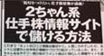
週刊SPA!7/24・31合併号のマネー(得)総本部のコーナーで当サイト『恐るべき注目銘柄株速報』のインタビュー記事が掲載されました。

週刊SPA!7/24・31合併号

blog_parts_sample

※このブログパーツは株ブログパーツページより無料配布中です

新着レス:

hide

top