【4427】EduLab【エデュ】
1 : 管理人 : 2018/11/20(火) 03:40:03 ID:OwnerKabu685
[特色]-
[連結事業]-
現在書き込みはありません。
EduLabを保有している方や思惑のある方は、ぜひ書き込みして行ってください!
EduLabの銘柄情報はコチラ→4427
[4427]EduLab 2ch&Yahoo板統合 新着口コミ情報
※コメントは常に更新されます
Yahoo掲示板(Y板) - 4427より
451 :東芝の株主集団訴訟の…:2025/05/10(土)14:36:00 ID:Destiny
Yahoo掲示板(Y板) - 4427より
450 :何らかの思惑が有れば…:2025/05/08(木)22:16:00 ID:ストップ高ライト
何らかの思惑が有れば飛びやすいんだけど、とりあえず業績相場に期待しますか。ノンホルです。
Yahoo掲示板(Y板) - 4427より
449 :ありがとうございまし…:2025/05/08(木)19:20:00 ID:hap*****
ありがとうございました。
Yahoo掲示板(Y板) - 4427より
448 :毎回、:2025/05/08(木)18:14:00 ID:ちくわ
毎回、決算発表の日時については公式に発表されません ただし、例年5月15日に発表されています これまでは3時に発表でしたが、取引時間の変更に伴い変更されたようで4時or4時半あたりになると思います
Yahoo掲示板(Y板) - 4427より
447 :決算日は何時でしょう…:2025/05/08(木)12:33:00 ID:hap*****
決算日は何時でしょうか?
Yahoo掲示板(Y板) - 4427より
446 :時価総額と出来高が小…:2025/05/07(水)13:07:00 ID:ちくわ
時価総額と出来高が小さいので上がるときは、爆上げするよ〰 今、爆上げの前兆現象がおきてるよ〰 待ってたら乗り遅れちゃうよ〰
Yahoo掲示板(Y板) - 4427より
445 :ちょっとここは面白い…:2025/05/07(水)11:08:00 ID:フレディ
ちょっとここは面白い動きしてるな。ただまだ今は買いじゃない。買うとすれば250円を切った時かな?
Yahoo掲示板(Y板) - 4427より
444 :好材料出た???!!…:2025/05/02(金)09:26:00 ID:86ue2500
好材料出た???!!
Yahoo掲示板(Y板) - 4427より
443 :材料出た???!!:2025/05/02(金)09:18:00 ID:86ue2500
材料出た???!!
Yahoo掲示板(Y板) - 4427より
441 :だからか:2025/05/01(木)13:36:00 ID:の(返信見ません)
だからか
【速報】急騰・急落銘柄報告スレ18287 より
947 :山師さん@トレード中 :2025/05/01(木)08:47:25 ID:3Yv4c/Ex0
エデュラボ見たいにプライムに居ればグロース落ちで許された可能性もあるが今現在グロースなので終わりだね(´・ω・`)
Yahoo掲示板(Y板) - 4427より
440 :誰も注目していないけ…:2025/04/30(水)15:55:00 ID:ちくわ
誰も注目していないけど、爆上げするよw 買われ方が不自然だよ 説得力はないがwww
【速報】急騰・急落銘柄報告スレ18277 より
761 :山師さん@トレード中 :2025/04/25(金)16:21:07 ID:alhKlaaB0
令和7年4月25日
金融庁
(株)EduLabにおける有価証券報告書等の虚偽記載に対する課徴金納付命令の決定について
https://www.fsa.go.jp/news/r6/shouken/20250425-1.html
「納付すべき課徴金の額 金2億3705万5000円」
【急騰】今買えばいい株22225【夥】 より
880 :山師さん:2025/04/24(木)22:55:01 ID:1UBgjo8L
🚨Trump is scheduled to talk around 12-1PM today.
【急騰】今買えばいい株22216【寄りチン】 より
373 :山師さん:2025/04/23(水)09:47:18 ID:Mbw6agYz
よりにもよってエデュラボかよお~
【急騰】今買えばいい株22216【寄りチン】 より
345 :山師さん:2025/04/23(水)09:44:07 ID:8sNJoaO/
Edulabきてる
【急騰】今買えばいい株22208【団鬼六】 より
536 :山師さん:2025/04/21(月)22:53:54 ID:fbXSdLse
Amid Trump’s tariffs, TSMC has been stepping up its investment in the U.S. According to Economic Daily News, the company is accelerating the timeline for its second Arizona fab. In addition, TSMC is reportedly set to introduce its latest fan-out panel-level packaging (FOPLP) technology in the U.S. to meet rising demand from customers seeking chips manufactured in the U.S.
The report highlights that, following major clients such as Apple, NVIDIA, and AMD announcing plans to expand their investments in the U.S., TSMC has accordingly adjusted its strategies.
TSMC is currently in its quiet period ahead of its earnings call and is unable to comment, as the report notes.
TSMC Advances FOPLP Technology
Citing Nikkei, the report states that TSMC is finalizing the specifications for its FOPLP technology in an effort to accelerate its mass production timeline. The first-generation version is expected to adopt a 300mm x 300mm panel size—smaller than the previously tested 510mm x 515mm format. According to the report, TSMC is currently building a pilot production line in Taoyuan, Taiwan, with limited trial production anticipated to begin as early as 2027.
The report also notes that TSMC initially explored partnering with panel makers such as Innolux but ultimately opted to develop the technology in-house, as the current precision and technical capabilities of the panel industry were deemed insufficient to meet TSMC’s standards.
As noted by the report, FOPLP offers improved heat dissipation compared to 3D stacking techniques such as wafer-on-wafer (WoW), CoWoS, and SoIC. However, its production efficiency is lower than that of existing 3D stacking methods. The report adds that AI customers are still expected to be the primary adopters of this packaging technology.
Tech Giants Fuel TSMC’s U.S. Manufacturing Expansion
Notably, on April 15, AMD CEO Lisa Su confirmed that the company is ramping up U.S. production. According to Reuters, AMD’s flagship chips will soon roll off TSMC’s new Arizona line—marking the first time its products will be manufactured in the U.S.
Meanwhile, NVIDIA recently also revealed plans to invest up to USD 500 billion in U.S.-based AI server production over the next four years and confirmed that its Blackwell chips are now being produced at TSMC’s Phoenix plant, as Reuters notes.
As noted by Economic Daily News, sources indicate that in response to requests from major clients such as AMD and Apple, TSMC has reportedly informed suppliers that equipment move-in for its second Arizona fab will begin as early as September this year—one full year ahead of schedule.
In other words, the fab’s 3nm production is now expected to begin by the end of 2027, while the second-phase line for 2nm is projected to enter mass production in 2028 as the report points out.
547 :山師さん:2025/04/21(月)23:01:35 Rfp0DKa2
>>536
荒らすなボケ!
【急騰】今買えばいい株22208【団鬼六】 より
528 :山師さん:2025/04/21(月)22:51:37 ID:HQwTJw7C
Amid Trump’s tariffs, TSMC has been stepping up its investment in the U.S. According to Economic Daily News, the company is accelerating the timeline for its second Arizona fab. In addition, TSMC is reportedly set to introduce its latest fan-out panel-level packaging (FOPLP) technology in the U.S. to meet rising demand from customers seeking chips manufactured in the U.S.
The report highlights that, following major clients such as Apple, NVIDIA, and AMD announcing plans to expand their investments in the U.S., TSMC has accordingly adjusted its strategies.
TSMC is currently in its quiet period ahead of its earnings call and is unable to comment, as the report notes.
TSMC Advances FOPLP Technology
Citing Nikkei, the report states that TSMC is finalizing the specifications for its FOPLP technology in an effort to accelerate its mass production timeline. The first-generation version is expected to adopt a 300mm x 300mm panel size—smaller than the previously tested 510mm x 515mm format. According to the report, TSMC is currently building a pilot production line in Taoyuan, Taiwan, with limited trial production anticipated to begin as early as 2027.
The report also notes that TSMC initially explored partnering with panel makers such as Innolux but ultimately opted to develop the technology in-house, as the current precision and technical capabilities of the panel industry were deemed insufficient to meet TSMC’s standards.
As noted by the report, FOPLP offers improved heat dissipation compared to 3D stacking techniques such as wafer-on-wafer (WoW), CoWoS, and SoIC. However, its production efficiency is lower than that of existing 3D stacking methods. The report adds that AI customers are still expected to be the primary adopters of this packaging technology.
Tech Giants Fuel TSMC’s U.S. Manufacturing Expansion
Notably, on April 15, AMD CEO Lisa Su confirmed that the company is ramping up U.S. production. According to Reuters, AMD’s flagship chips will soon roll off TSMC’s new Arizona line—marking the first time its products will be manufactured in the U.S.
Meanwhile, NVIDIA recently also revealed plans to invest up to USD 500 billion in U.S.-based AI server production over the next four years and confirmed that its Blackwell chips are now being produced at TSMC’s Phoenix plant, as Reuters notes.
As noted by Economic Daily News, sources indicate that in response to requests from major clients such as AMD and Apple, TSMC has reportedly informed suppliers that equipment move-in for its second Arizona fab will begin as early as September this year—one full year ahead of schedule.
In other words, the fab’s 3nm production is now expected to begin by the end of 2027, while the second-phase line for 2nm is projected to enter mass production in 2028 as the report points out.
【急騰】今買えばいい株22208【団鬼六】 より
527 :山師さん:2025/04/21(月)22:51:14 ID:N5bUdpKO
Amid Trump’s tariffs, TSMC has been stepping up its investment in the U.S. According to Economic Daily News, the company is accelerating the timeline for its second Arizona fab. In addition, TSMC is reportedly set to introduce its latest fan-out panel-level packaging (FOPLP) technology in the U.S. to meet rising demand from customers seeking chips manufactured in the U.S.
The report highlights that, following major clients such as Apple, NVIDIA, and AMD announcing plans to expand their investments in the U.S., TSMC has accordingly adjusted its strategies.
TSMC is currently in its quiet period ahead of its earnings call and is unable to comment, as the report notes.
TSMC Advances FOPLP Technology
Citing Nikkei, the report states that TSMC is finalizing the specifications for its FOPLP technology in an effort to accelerate its mass production timeline. The first-generation version is expected to adopt a 300mm x 300mm panel size—smaller than the previously tested 510mm x 515mm format. According to the report, TSMC is currently building a pilot production line in Taoyuan, Taiwan, with limited trial production anticipated to begin as early as 2027.
The report also notes that TSMC initially explored partnering with panel makers such as Innolux but ultimately opted to develop the technology in-house, as the current precision and technical capabilities of the panel industry were deemed insufficient to meet TSMC’s standards.
As noted by the report, FOPLP offers improved heat dissipation compared to 3D stacking techniques such as wafer-on-wafer (WoW), CoWoS, and SoIC. However, its production efficiency is lower than that of existing 3D stacking methods. The report adds that AI customers are still expected to be the primary adopters of this packaging technology.
Tech Giants Fuel TSMC’s U.S. Manufacturing Expansion
Notably, on April 15, AMD CEO Lisa Su confirmed that the company is ramping up U.S. production. According to Reuters, AMD’s flagship chips will soon roll off TSMC’s new Arizona line—marking the first time its products will be manufactured in the U.S.
Meanwhile, NVIDIA recently also revealed plans to invest up to USD 500 billion in U.S.-based AI server production over the next four years and confirmed that its Blackwell chips are now being produced at TSMC’s Phoenix plant, as Reuters notes.
As noted by Economic Daily News, sources indicate that in response to requests from major clients such as AMD and Apple, TSMC has reportedly informed suppliers that equipment move-in for its second Arizona fab will begin as early as September this year—one full year ahead of schedule.
In other words, the fab’s 3nm production is now expected to begin by the end of 2027, while the second-phase line for 2nm is projected to enter mass production in 2028 as the report points out.
【急騰】今買えばいい株22208【団鬼六】 より
526 :山師さん:2025/04/21(月)22:51:03 ID:+p5wlGn+
Amid Trump’s tariffs, TSMC has been stepping up its investment in the U.S. According to Economic Daily News, the company is accelerating the timeline for its second Arizona fab. In addition, TSMC is reportedly set to introduce its latest fan-out panel-level packaging (FOPLP) technology in the U.S. to meet rising demand from customers seeking chips manufactured in the U.S.
The report highlights that, following major clients such as Apple, NVIDIA, and AMD announcing plans to expand their investments in the U.S., TSMC has accordingly adjusted its strategies.
TSMC is currently in its quiet period ahead of its earnings call and is unable to comment, as the report notes.
TSMC Advances FOPLP Technology
Citing Nikkei, the report states that TSMC is finalizing the specifications for its FOPLP technology in an effort to accelerate its mass production timeline. The first-generation version is expected to adopt a 300mm x 300mm panel size—smaller than the previously tested 510mm x 515mm format. According to the report, TSMC is currently building a pilot production line in Taoyuan, Taiwan, with limited trial production anticipated to begin as early as 2027.
The report also notes that TSMC initially explored partnering with panel makers such as Innolux but ultimately opted to develop the technology in-house, as the current precision and technical capabilities of the panel industry were deemed insufficient to meet TSMC’s standards.
As noted by the report, FOPLP offers improved heat dissipation compared to 3D stacking techniques such as wafer-on-wafer (WoW), CoWoS, and SoIC. However, its production efficiency is lower than that of existing 3D stacking methods. The report adds that AI customers are still expected to be the primary adopters of this packaging technology.
Tech Giants Fuel TSMC’s U.S. Manufacturing Expansion
Notably, on April 15, AMD CEO Lisa Su confirmed that the company is ramping up U.S. production. According to Reuters, AMD’s flagship chips will soon roll off TSMC’s new Arizona line—marking the first time its products will be manufactured in the U.S.
Meanwhile, NVIDIA recently also revealed plans to invest up to USD 500 billion in U.S.-based AI server production over the next four years and confirmed that its Blackwell chips are now being produced at TSMC’s Phoenix plant, as Reuters notes.
As noted by Economic Daily News, sources indicate that in response to requests from major clients such as AMD and Apple, TSMC has reportedly informed suppliers that equipment move-in for its second Arizona fab will begin as early as September this year—one full year ahead of schedule.
In other words, the fab’s 3nm production is now expected to begin by the end of 2027, while the second-phase line for 2nm is projected to enter mass production in 2028 as the report points out.
【急騰】今買えばいい株22208【団鬼六】 より
521 :山師さん:2025/04/21(月)22:50:11 ID:rwHZuuRz
Amid Trump’s tariffs, TSMC has been stepping up its investment in the U.S. According to Economic Daily News, the company is accelerating the timeline for its second Arizona fab. In addition, TSMC is reportedly set to introduce its latest fan-out panel-level packaging (FOPLP) technology in the U.S. to meet rising demand from customers seeking chips manufactured in the U.S.
The report highlights that, following major clients such as Apple, NVIDIA, and AMD announcing plans to expand their investments in the U.S., TSMC has accordingly adjusted its strategies.
TSMC is currently in its quiet period ahead of its earnings call and is unable to comment, as the report notes.
TSMC Advances FOPLP Technology
Citing Nikkei, the report states that TSMC is finalizing the specifications for its FOPLP technology in an effort to accelerate its mass production timeline. The first-generation version is expected to adopt a 300mm x 300mm panel size—smaller than the previously tested 510mm x 515mm format. According to the report, TSMC is currently building a pilot production line in Taoyuan, Taiwan, with limited trial production anticipated to begin as early as 2027.
The report also notes that TSMC initially explored partnering with panel makers such as Innolux but ultimately opted to develop the technology in-house, as the current precision and technical capabilities of the panel industry were deemed insufficient to meet TSMC’s standards.
As noted by the report, FOPLP offers improved heat dissipation compared to 3D stacking techniques such as wafer-on-wafer (WoW), CoWoS, and SoIC. However, its production efficiency is lower than that of existing 3D stacking methods. The report adds that AI customers are still expected to be the primary adopters of this packaging technology.
Tech Giants Fuel TSMC’s U.S. Manufacturing Expansion
Notably, on April 15, AMD CEO Lisa Su confirmed that the company is ramping up U.S. production. According to Reuters, AMD’s flagship chips will soon roll off TSMC’s new Arizona line—marking the first time its products will be manufactured in the U.S.
Meanwhile, NVIDIA recently also revealed plans to invest up to USD 500 billion in U.S.-based AI server production over the next four years and confirmed that its Blackwell chips are now being produced at TSMC’s Phoenix plant, as Reuters notes.
As noted by Economic Daily News, sources indicate that in response to requests from major clients such as AMD and Apple, TSMC has reportedly informed suppliers that equipment move-in for its second Arizona fab will begin as early as September this year—one full year ahead of schedule.
In other words, the fab’s 3nm production is now expected to begin by the end of 2027, while the second-phase line for 2nm is projected to enter mass production in 2028 as the report points out.
【急騰】今買えばいい株22208【団鬼六】 より
23 :山師さん:2025/04/21(月)18:12:44 ID:flJud41f
4427ご発注かも持ってるヤツ急げ
【急騰】今買えばいい株22188【妖艶デヴィ夫人】 より
166 :山師さん:2025/04/16(水)12:37:48 ID:7G67uB2C
エデュラボか?
続きは4427銘柄情報ページでご確認ください
掲示板書き込み
- スパム対策の為、URLは"h"を抜いた"ttp"から入力して下さい。
- 宣伝目的と思われる書き込みに記載されたURLにはサイト内銘柄ページ、ブログランキング他、当サイトからのリンクを全て除外させて頂きます。
銘柄別掲示板一覧
- 【3475】 グッドコムアセット(1)
- 【9468】 KADOKAWA(1)
- 【2120】 LIFULL(1)
- 【6743】 大同信号(5)
- 【2330】 フォーサイド(1)
- 【6301】 コマツ(2)
- 【3686】 ディー・エル・イー(1)
- 【2767】 円谷フィールズホールディングス(1)
- 【3399】 丸千代山岡家(1)
- 【3133】 海帆(1)
- 【8226】 理経(5)
- 【6966】 三井ハイテック(1)
- 【9504】 中国電力(1)
- 【2764】 ひらまつ(37)
- 【9558】 ジャパニアス(1)
- 【2370】 メディネット(10)
- 【3401】 帝人(3)
- 【2418】 ツカダ・グローバルホールディング(1)
- 【2157】 コシダカホールディングス(1)
- 【3099】 三越伊勢丹ホールディングス(1)
- 【8233】 高島屋(1)
- 【6191】 エアトリ(1)
- 【7554】 幸楽苑(1)
- 【3030】 ハブ(1)
- 【3481】 三菱地所物流リート投資法人(1)
- 【3907】 シリコンスタジオ(20)
- 【3470】 マリモ地方創生リート投資法人(1)
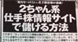
- 【6753】 シャープ(9)
- 【2698】 キャンドゥ(1)
- 【3940】 ノムラシステムコーポレーション(1)
東芝の株主集団訴訟の判決、個人株主集団(原告)勝訴のようだ?ここの係争中裁判判決、その悪質性は同等もしくはそれ以上と思うので予測できそうダ?